
Conditioning A/V Signals for RF Modulation
The circuit design for the audio and video signal conditioning involves several key components to ensure compatibility with RF modulator inputs. The audio path starts with a lowpass filter, specifically designed to attenuate frequencies above the desired range, thus preventing aliasing and ensuring a clean signal. The choice of a -3dB point between 22kHz and 24kHz is critical, as it aligns with typical audio bandwidth requirements while allowing sufficient headroom for audio peaks.
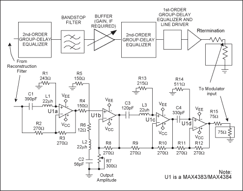
For the video signal, the implementation of a three-pole reconstruction filter is essential. This filter configuration provides the necessary attenuation of high-frequency components and ensures that the output signal adheres to the specifications outlined in ITU-R BT. 470-6. The design of this filter requires careful consideration of component values to achieve the desired cutoff frequency and phase response, minimizing group-delay variations that can lead to synchronization issues in the modulated output.
In addition to filtering, operational amplifiers (op-amps) play a crucial role in signal amplification and level adjustment. The op-amps must be selected based on their bandwidth, noise characteristics, and ability to drive the necessary loads without distortion. The use of feedback networks in conjunction with these op-amps allows for fine-tuning of gain and stability in the audio and video paths.
The integration of notch filters in the design is particularly important for addressing potential interference from the audio subcarrier. By strategically placing these filters within the circuit, it is possible to significantly reduce group-delay variations and improve overall signal integrity. The implementation of these filters requires precise tuning to ensure that they effectively target the subcarrier frequency without adversely affecting the surrounding frequency spectrum.
Overall, the discrete design approach allows for greater flexibility in meeting the varying requirements of different modulator standards. By utilizing standard components such as op-amps and passive filters, the resulting circuit can be tailored to specific applications while maintaining cost-effectiveness. This adaptability is particularly beneficial in environments where multiple A/V sources may be connected, ensuring that high-quality RF-modulated outputs are consistently achieved.Even as display devices move toward digital video, they retain the legacy of an RF-modulated analog TV output. That output is specified in the US by the National Television Standards Committee (NTSC), and utilized in security applications and in the Digital Video Broadcasting (DVB) Project as specified by the European TV standard phase al
ternation line (PAL). All modulators, whether simple analog types or single-chip synthesizers, require properly conditioned audio and video input signals. Despite the need for an integrated circuit, the ubiquitous interface between the modulator and audio/video (A/V) signals has not yet been reduced to an IC.
The main reasons for that deficiency are the difficulty of such a design, the variations required for different standards, and the variable levels required by the modulator itself. The alternative to an IC interface is a discrete design. The signal-conditioning requirements include lowpass and notch filtering of the video, group-delay compensation for the video, preemphasis for the audio, and (to adjust the modulation level) level controls for both audio and video.
Because many cable and satellite receivers, VCRs, DVDs, and TVs do not fully comply with these signal-conditioning requirements, the modulated signals of channels 3 and 4 have poorer quality than that of the baseband composite (Cvbs). The following discussion explains the interface requirements and how to meet them using standard op amps and discrete components.
The resulting low-cost circuitry can also provide rear-panel outputs for most A/V appliances. For driving RF modulators in NTSC and PAL systems, the allowable video group-delay variation and required audio preemphasis are clearly specified by Recommendation ITU-R BT. 470-6. Most of the other indistinct specifications are summarized and extrapolated to include other, unstated design specifications in Tables 1 and 2.
Table content is based on typical back-panel outputs for a TV, DVD, or set-top box having both baseband and RF-modulated A/V outputs (Figure 1). Some of these requirements depend on the source. If the signals to the modulator come from a DAC, for example, they obviously need reconstruction filtering to prevent out-of-band modulation, and to remove artifacts, noise, and aliased signals.
Generally, they must also be amplified to compensate for back-terminated loads and variation in the DAC outputs. The requirement to notch-filter the video around the audio subcarrier is not stated, but implied by the group-delay adjustment described in Figure 3 of ITU-R BT.
470-6. Such notch filtering is usually recommended for modulator chips. Also requiring attenuation are the rear-panel signals, whose output levels are typically higher than required for the modulator inputs. These conditions lead to requirements for the A/V interface of Figure 1: A sound-subcarrier bandstop or notch filter, centered on the sound subcarrier; this filtering causes a large variation in group delay near the notch frequency The first thing to be done is lowpass-reconstruction filtering to suppress aliased outputs and out-of-band noise in the modulator`s audio and video inputs.
Active filters for that purpose allow the increase of the DAC output to standard levels, while driving the rear panel and the RF modulator. Audio adjustment requires a lowpass filter (LPF) with a -3dB point of 22kHz to 24kHz, and enough gain to produce 2VRMS at the rear panel.
We assume a gain of two and, because audio is highly oversampled, the requirement can be met with a single passive RC filter. As explained later, the second RC filter is for the audio modulator, not reconstruction. The Figure 2 circuit drives the rear-panel outputs and the input to the audio portion of the RF modulator.
Video adjustment is more difficult. It is not highly oversampled and, therefore, requires at least a three-pole reconstruction filter. If this filter causes exces 🔗 External reference
Related Circuits
This circuit filters noise, such as glitches and contact bounce, from digital signals. It can be easily adjusted for a wide range of noise frequencies. The circuit's output changes state only if the input differs from the output long...
This is a coincidence detector circuit. This circuit is very useful for monitoring complex logic circuits. This circuit has two inputs, A and B. If A and B are... The coincidence detector circuit is designed to identify when two input...
This circuit is an Automatic Gain Control (AGC) system designed for audio-frequency signals. AGC systems typically consist of three main components: an amplifier, a rectifier, and a controlled impedance. In this particular circuit, the functions of both the amplifier...
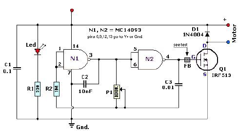
A quad 2-input NAND Schmitt trigger circuit can be designed using the MC14093 CMOS type IC, which serves as a simple pulse width modulation (PWM) controller electronic project. This PWM controller is straightforward and requires only a few external...
A 1997 Ford Thunderbird experienced a failure of the blower/fan when the air conditioning was activated, accompanied by a snapping sound under the instrument panel. This resulted in no airflow for the air conditioning, heater, or defrost functions. The...
Commercial FM demodulation occurs at an intermediate frequency (IF) of 10.7 MHz. With a frequency deviation of ±75 kHz, the deviation of the IF carrier is approximately ±0.7%. This deviation allows for the conversion of FM to AM or...