
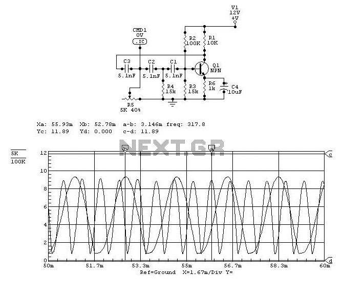
Data control variable frequency oscillator
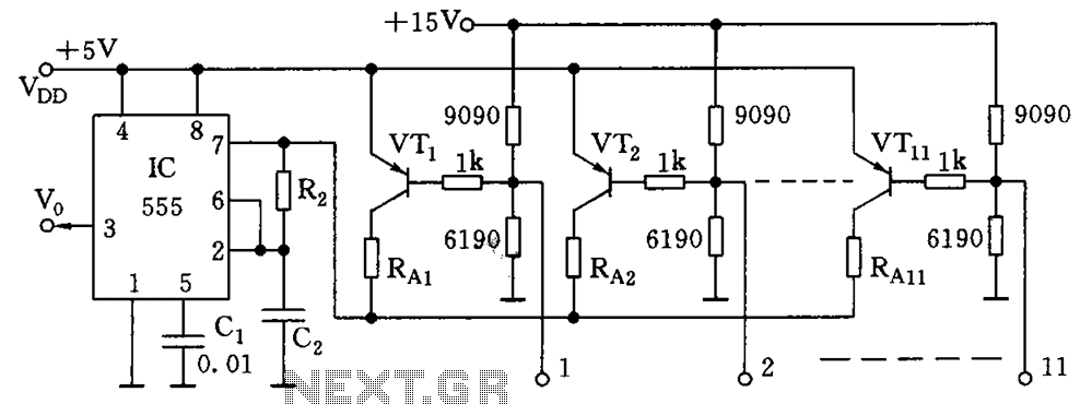
The described circuit employs a base biasing technique for a series of bipolar junction transistors (BJTs) labeled VT1 through VT11. Each transistor is configured to respond to a binary input signal, facilitating the generation of a corresponding output based on the binary state. The circuit can handle a total of 2048 unique combinations, as indicated by the 11 bits utilized in the configuration.
When a binary input is low (0), the associated transistor (VT) is activated, creating a conductive path that allows current to flow through the circuit. This activation causes capacitor C2 to charge via the resistors RA and R2. The charging process is influenced by the values of these resistors, where RA provides an equivalent resistance that determines the time constant of the charging circuit. The time constant, in turn, plays a critical role in defining the oscillation frequency of the circuit, which is essential for applications requiring precise timing and switching characteristics.
The overall functionality of this circuit is crucial in digital applications where binary data needs to be processed and converted into corresponding analog signals or other digital states. The careful selection of resistor values and capacitor characteristics ensures optimal performance, stability, and reliability in various electronic systems. This design can be implemented in applications such as signal processing, data communication, and control systems where binary state representation and manipulation are fundamental. As shown in FIG, VT1 ~ VT11 base bias circuit 11 added to the binary data (high level 1 to low level 0 ), there are 211 2048 combinations. When a bit is low, the corresponding VT turns on, the C2 by RA + R2 charging it, RA conducting pipe for the equivalent resistance of the resistor, the oscillation frequency
Related Circuits
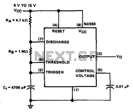
The NE555 timer is configured in astable mode and utilizes three timing components (RA, RB, and Ct). A 0.01 µF bypass capacitor is connected to pin 5 to enhance noise immunity. The operational limitations of the astable mode are...

This is a simple automatic light switch circuit designed for bedrooms. After construction, connect the input terminals of this circuit in parallel to the existing light fixture. The automatic light switch circuit operates using a photoresistor (LDR) and a transistor...
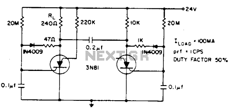
Electrolytic capacitors are not required to generate a 1 cps frequency. When the silicon-controlled switch (SCS) is triggered, the 0.2 µF commutating capacitor deactivates the other capacitor and charges its gate capacitor to a negative potential. The gate capacitor...
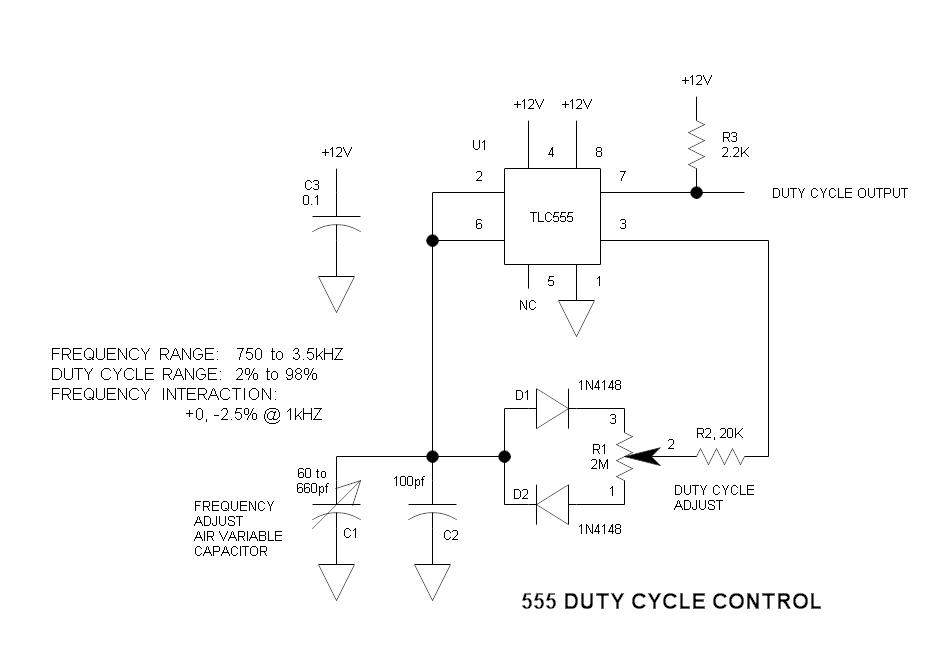
This is a simple oscillator circuit that varies the duty cycle over a wide range without affecting the frequency. It is a variation of the simple 555 astable multivibrator. The oscillator circuit utilizes the 555 timer IC configured in astable...
Another application of the frequency-to-voltage converter (FVC) is the tone/frequency decoder. This circuit is designed to identify the frequency band of an oscillating signal. It is utilized in various applications, such as determining the frequency band in signals and...
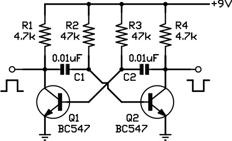
This circuit is one of the simplest to implement but can be challenging to comprehend. It consists of a two-transistor oscillator known as an astable multivibrator, which generates a square wave output that is out of phase. Initially, it...
Warning: include(partials/cookie-banner.php): Failed to open stream: Permission denied in /var/www/html/nextgr/view-circuit.php on line 713
Warning: include(): Failed opening 'partials/cookie-banner.php' for inclusion (include_path='.:/usr/share/php') in /var/www/html/nextgr/view-circuit.php on line 713