
Dc-gain-controlled-video-amplifier
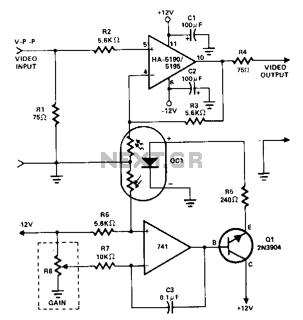
This amplifier utilizes a cascaded operational amplifier (op amp) integrator and a transistor buffer, Q1, to drive the gain control element. With a minor modification, the HA-5190/5195 stage is configured as a conventional non-inverting op amp and includes input and output impedance matching resistors R1 and R4, respectively, a series stabilization resistor RZ, and power supply bypass capacitors C1 and C2. The circuit is distinct from standard designs as the gain control network incorporates a photoresistor, part of the optocoupler (OC1). The optocoupler contains two matched photoresistors, both activated by a common LED.
The effective resistances of these devices are inversely proportional to the light emitted by the LED. One photoresistor is part of the HA-5190/5195 gain network, in conjunction with R3, while the other forms a voltage divider with R6 to control the bias applied to the integrator's non-inverting terminal. During operation, the DC voltage supplied by the gain control resistor R8 is applied to the integrator's inverting input terminal through input resistor R7. Depending on the relative magnitude of the control voltage, the integrator output will either charge or discharge capacitor C3. This change in output, amplified by Q1, regulates the current supplied to the OC1 LED through series limiting resistor R5. The process continues until the voltage applied to the integrator's non-inverting input by the R6-photoresistor gain network varies, adjusting the gain of the op amp stage. As the control voltage at R8 is modified, the photoresistances of OC1 track these changes, automatically readjusting the op amp in accordance with the new control voltage setting.
This amplifier circuit is designed to provide a dynamic gain control mechanism through the integration of an optocoupler and a feedback loop involving a photoresistor. The cascaded op amp integrator serves as the primary signal processing unit, where the gain is adjusted based on the illumination provided by the LED within the optocoupler. The circuit's architecture ensures that variations in control voltage at R8 directly affect the output of the integrator, which in turn modifies the current flowing through the LED, thereby influencing the photoresistor's resistance.
The inclusion of resistors R1, R4, RZ, R3, R6, and R7 ensures proper impedance matching and stabilization of the circuit, facilitating optimal performance of the op amp stage. Capacitors C1 and C2 are critical for power supply decoupling, providing stability against voltage fluctuations. The feedback mechanism, which relies on the photoresistor's response to the LED's output, allows for a smooth and continuous adjustment of the amplifier's gain, making this design suitable for applications requiring precise control over amplification levels.
In summary, this circuit exemplifies a sophisticated approach to gain control in amplifiers, leveraging the properties of optoelectronic components to achieve automatic adjustments in response to varying input conditions. The design is well-suited for applications in audio processing, signal conditioning, and other fields where adaptive gain control is essential.This amplifier employs a cascaded op amp integrator and transistor buffer, Q1, to drive the gain control element. Except for a simple modification, the HA-5190/5195 stage is connected as a conventional noninverting op amp, and includes input and output impedance matching resistors R1 and R4, respectively, series stabilization resistor RZ, and power supply bypass capacitors C1 and C2.
The circuit differs from standard designs in that the gain control network includes a photoresistor, part of OCl. The optocoupler/isolator OC1 contains two matched photoresistors, both activated by a common LED. The effective resistances offered by these devices are inversely proportional to the light emitted by the LED. Onephotoresistor is part, with R3, of the HA-5190/5195 gain network, while the other forms a voltage-divider with R6 to control the bias applied to the integrator noninverting terminal.
In operation, the de voltage supplied by gain control R8 is applied to the integrator inverting input terminal through input resistor R7. Depending on the relative magnitude of the control voltage, the integrator output will either charge or discharge C3.
This change in output, amplified by Q1, controls the current supplied to the OC 1 LED through series limiting resistor R5. The action continues until the voltage applied to the integrator noninverting input by the R6-photoresistor gain network is changing, adjusting the op amp stage gain.
As the control voltage at R8 is readjusted, the OC1 photoresistances track these changes, automatically readjusting the op amp in accordance with the new control voltage setting. 🔗 External reference