dc-voltage-doubler.html

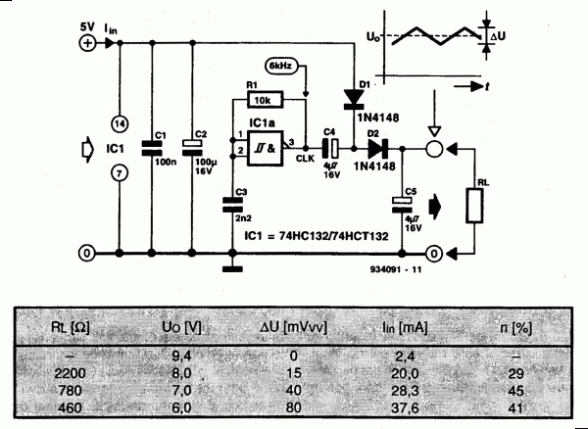
The circuit of the DC Voltage Doubler was designed for a specific type of power supply. It is important to study the schematic design and accompanying photographs of the DC Voltage Doubler circuit to understand the components involved. This economical DC Voltage Doubler circuit diagram requires very few components and is capable of producing 10V from a 5V power supply. If an oscillator is necessary, it can be built using a non-functional gate, which will require two additional components: R1 and C3. The main parameters of this voltage doubler circuit are provided below. It should be noted that due to IC tolerances, these values may vary. This article discusses the DC Voltage Doubler, and more articles can be found at the provided URL. Sharing or copying this article is allowed, but the source link must be included.
The DC Voltage Doubler circuit is a fundamental electronic design that enhances the voltage level of a DC power supply. The circuit typically employs a combination of capacitors and diodes to achieve voltage doubling. In this specific design, the circuit is capable of converting a 5V input into a 10V output, making it particularly useful for applications where higher voltage levels are required from a limited power supply.
The primary components of the circuit include two diodes and two capacitors. The diodes are arranged in such a way that they allow current to flow in one direction while blocking it in the opposite direction, effectively charging the capacitors to double the input voltage. The capacitors store charge during the positive half cycle of the input voltage, and then, during the negative half cycle, they discharge through the load, providing a higher voltage output.
In scenarios where an oscillator is necessary, a non-functional gate can be utilized to generate the required switching signals. This additional circuitry introduces two more components, R1 (a resistor) and C3 (an additional capacitor), which assist in stabilizing the oscillation and ensuring proper operation of the voltage doubler.
It is important to note that the performance of the voltage doubler may vary based on the tolerances of the integrated circuits used. Therefore, careful consideration of component specifications is essential to achieve the desired output voltage reliably. The design is not only efficient but also cost-effective, making it suitable for various applications in electronics where space and component count are critical factors.The The Circuit of DC Voltage Doubler was designed on arrived type Power Supply. Please study carefully and comprehend by the side of schematic design photos of The Circuit of DC Voltage Doubler to pick up factor in sequence. This is a economical DC Voltage Doubler Circuit diagram, which requires a hardly any components and strength of character s
urrender 10V from a 5V power supply. If the oscillator essential be present built from a non-functional gate next is essential 2 supplementary components: R1 and C3. The a large amount principal parameters of this voltage doubler circuit are set arrived the submit less than.
memorandum with the aim of as of the IC tolerances these data may possibly contain approximately differences. You are reading the article about DC Voltage Doubler and you can find articles DC Voltage Doubler this the url.
You may distribute or copy articles DC Voltage Doubler this is beneficial if you or your friends, but do not forget to include the link source. 🔗 External reference