Debouncing Switches
1. What is Switch Debouncing?
1.1 What is Switch Debouncing?
Switch debouncing refers to the process of eliminating the spurious signals that occur when a mechanical switch is pressed or released. When a switch is activated, the physical contacts do not make a clean, instantaneous transition between states. Instead, they can 'bounce', resulting in several rapid on/off cycles before stabilizing in one position. This undesirable behavior can introduce errors in digital circuits and lead to unintended signals being processed by microcontrollers or digital logic.
To understand the underlying mechanics of switch debouncing, we must first consider the physical properties of mechanical switches. Most switches utilize metallic contacts that can inherently experience minor vibrations and oscillations upon actuation. This mechanical instability leads to the phenomenon known as contact bounce. The bouncing duration is typically on the order of tens to hundreds of milliseconds, which is significant enough to impact system performance, particularly in high-speed applications.
The inherent difficulty of processing these bouncing signals lies in the differing voltage levels produced during these transitions. As shown in the accompanying figure, when a switch connects or disconnects, several transitions can occur due to the bouncy nature of the mechanical contacts. If the switch is connected to a digital input pin of a microcontroller, the signal could be interpreted as rapidly toggling between high and low states, potentially leading to erratic behavior and faulty logic interpretation.
From a practical standpoint, debouncing is crucial in various applications, including keyboard inputs, user interface buttons, and any scenario where reliable binary feedback is necessary. Engineers commonly implement both hardware and software solutions to achieve effective debouncing.
Hardware Debouncing Techniques
A typical hardware approach involves adding components such as resistors and capacitors to filter out the unwanted noise. For instance, a simple RC (resistor-capacitor) low-pass filter can smooth out the voltage ripple caused by bouncing. The time constant, defined as \( \tau = RC \), plays a crucial role in determining how quickly the circuit responds to a change in state while filtering out the noise. An ideal resistor-capacitor combination might give a rise time comparable to the bouncing duration, effectively filtering the unwanted oscillations.
Through careful selection of the resistor and capacitor values, the designer can adjust the cutoff frequency to suit the specific requirements of the application, thus ensuring a clean signal transition in the desired timeframe.
Software Debouncing Methods
On the software side, many microcontroller developers implement debouncing algorithms to handle switch inputs. A commonly used technique is to introduce a delay after the switch state changes. A pseudo-code example might look like this:
When the button state changes:
- Record the current state and timestamp.
- Wait for a predefined debounce period.
- If the switch state remains stable after the delay, accept the new state.
This method allows software to filter out the rapid transitions induced by bouncing, ensuring that only stable, intentional changes in state are registered.
In summary, switch debouncing is a fundamental concept in electronics that has significant implications for reliability and accuracy in digital systems. By understanding the mechanisms that contribute to contact bounce and employing effective debouncing strategies, engineers can enhance the performance of their circuits and systems.
1.2 The Importance of Debouncing in Circuits
In the context of electronic circuits, particularly those involving mechanical switches, debouncing plays a critical role in ensuring reliable operation. Mechanical switches, such as tactile buttons, typically generate noise or multiple transitions when actuated due to the physical contact bouncing between conductive surfaces. This phenomenon can lead to unintended consequences in digital circuits, misinterpreting rapid transitions as multiple presses rather than a single action.
Understanding the importance of debouncing is fundamental for designing robust systems. When a switch is activated, the bouncing can cause a microcontroller or logic circuit to register multiple inputs instead of one, potentially leading to erratic behavior or incorrect outputs. For example, in an audio control system, a user pressing a volume button could inadvertently raise or lower the sound level drastically due to a single press being interpreted as multiple actions.
The Mechanism of Electrical Noise
To comprehend the repercussions of switch bounce, it helps to analyze how mechanical contacts behave during actuation. When a switch is pressed:
- The contacts first touch, leading to an initial closure.
- Due to vibration and imperfections in the mechanical surfaces, the contacts may lose contact momentarily.
- This creates rapid on/off cycles that can last for a few milliseconds, resulting in electrical noise that propagates as unintended signals.
The duration and frequency of these bounces can vary significantly depending on the switch design and materials. Most bounces typically continue for about 5 to 30 milliseconds, indicating the immediate necessity for debouncing mechanisms in digital circuits.
Debouncing Solutions
There are primarily two approaches to implement debouncing: hardware and software solutions. Understanding when to use each can optimize system design.
Hardware Debouncing
Using additional electronic components—such as resistors, capacitors, or dedicated debouncing ICs—can effectively mitigate switch bounces. In hardware debouncing, a low-pass filter configuration smooths out the fluctuations. For example, a resistor-capacitor (RC) filter can be placed in parallel with the switch to allow errors in logic signaling to settle before the signal is read.
Software Debouncing
In microcontroller applications, debouncing can also be handled in software with techniques that involve timing delays or state machines. For instance, a software debouncing routine could ignore subsequent presses for a specified time frame (e.g., 50 milliseconds) after the first detected press. State transitions within an interrupt service routine can also be utilized to filter out uncertain readings effectively.
Implementing such solutions is not merely a design choice but a necessity for ensuring reliability in electronic devices ranging from simple controllers to complex embedded systems. Understanding the underlying causes of switch bounce and the methods to mitigate it opens pathways to designing smoother user experiences and more stable electronic systems.
By acknowledging the significance of debouncing in circuits, engineers and developers can improve product reliability, and avoid potential pitfalls associated with signal discrepancies. Through employing both hardware and software methods, professionals can tailor solutions specific to application requirements, ultimately leading to enhanced communication within the electronic circuit ecosystem.
1.3 Causes of Switch Bouncing
Understanding the phenomenon of switch bouncing is essential for engineers and researchers working with electronic systems, particularly in the design of robust input mechanisms. This section delves into the fundamental causes of switch bouncing, a common issue that arises during the mechanical operation of switches. Switch bouncing is primarily a mechanical and electrical phenomenon where the switch contacts may not settle into a stable state immediately upon actuation. Instead, they oscillate between making and breaking contact several times before stabilizing. The underlying mechanics of switch bouncing can be attributed to several factors, including mechanical resonance, material properties, and the structural design of the switch itself. Each of these factors contributes uniquely to the bouncing behavior, and understanding them allows for better design choices in reducing the impact of bounces on signal integrity.Mechanical Resonance
Mechanical resonance occurs when the mass and elasticity of the switch components interact. When a switch is actuated, the spring-loaded mechanism generates a force that can cause the contacts to vibrate at a specific frequency. This oscillation may lead to brief periods where the contacts repeatedly connect and disconnect. The resonance frequency can be estimated based on the spring constant and the mass of the moving parts:Material Properties
The materials used in switch construction significantly influence both the electrical and mechanical performance. For instance, the contact materials need to effectively conduct electricity while also providing adequate mechanical resilience. Common materials include gold, silver, and various alloys, each possessing unique characteristics regarding conductivity and adhesion. Wear and deformation of these materials can also lead to unpredictable bouncing behavior. The surface roughness and the sticking properties of different materials can cause variations in the time it takes for the contacts to stabilize after actuation, further complicating the bouncing phenomenon. Engineers must select materials that not only maximize conductivity but also minimize the likelihood of adhesion and wear.Structural Design Considerations
The design of the switch plays a crucial role in the bouncing behavior. Different types of switches—be it toggle, push button, or membrane switches—exhibit varying characteristics in their bounce behavior due to differences in their mechanical configurations. The geometry of the switch housing, the arrangement of contacts, and how the switch is mounted can all affect the bouncing duration. For example, a switch designed with a large surface area for contact may experience slower stabilization due to the mass of the contact and the forces involved in the spring mechanism. In contrast, a switch with a streamlined design may create a more direct path for the contacts to settle, reducing bounce time. Practical applications of understanding and mitigating switch bouncing include the design of keypads, voting systems, and user interfaces in electronic devices. Signal processing techniques and hardware debouncing methods, such as capacitor-based filters or dedicated debouncing ICs, are employed to ensure that switch activations result in reliable digital signals, thus enhancing the performance and usability of electronic systems. In summary, the causes of switch bouncing can be distilled into mechanical resonance, material properties, and structural design, each influencing the switch's performance during operation. By addressing these factors, engineers can create more effective debouncing strategies, leading to improved functionality in various electronic applications.2. Mechanical Debouncing Solutions
2.1 Mechanical Debouncing Solutions
The phenomenon of switch bounce occurs when a mechanical switch is actuated, leading to multiple unintended transitions between on and off states before settling into a stable state. This is a critical consideration in digital circuit design, as it can introduce errors in signal processing, leading to unpredictable behavior in applications such as microcontrollers, timers, and user interfaces. Understanding and implementing mechanical debouncing solutions is vital for ensuring reliability in electronic systems. To appreciate the solutions available, it's important to first examine the mechanism of bounce itself. When a switch is pressed, the electrical contacts may physically bounce against one another, resulting in rapid fluctuations between connectivity (on) and disconnection (off). These adjustments can persist for several milliseconds, typically in the range of 5 to 50 ms, depending on the materials and design of the switch. Different approaches exist to mitigate the effects of switch bounce, and we can categorize them broadly into two main categories: hardware and software solutions. In this subsection, we will concentrate on hardware-based mechanical debouncing solutions, which can be particularly advantageous in scenarios where software processing power is limited or real-time response is critical.Passive Debouncing Using RC Circuits
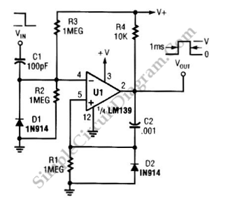
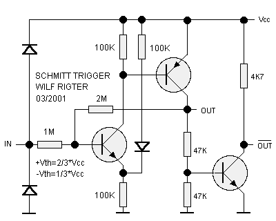
One of the simplest and most commonly used methods for mechanical switch debouncing is through the application of passive RC (Resistor-Capacitor) filtering. The basic principle involves using a resistor and capacitor in conjunction with the switch to create a low-pass filter that smoothens transitions. When the switch is pressed, the capacitor charges through the resistor, resulting in a gradual voltage rise instead of an abrupt change. This transition period effectively filters out any high frequency noise generated by the bouncing mechanism. The resistor-capacitor time constant \( \tau \) determines the rate at which the capacitor charges:Schmitt Trigger Circuits
Another effective mechanism for debouncing is the incorporation of a Schmitt Trigger. This component introduces hysteresis into the switching characteristics, creating distinct threshold voltages for the transition from LOW to HIGH and from HIGH to LOW. This means that once a threshold voltage is crossed, the output will only switch states after the voltage drops below a different threshold. The Schmitt Trigger configuration can be designed using discrete components such as operational amplifiers or could be integrated into logic circuits. The advantages include more robust noise immunity and a faster response time compared to passive filters.Practical Implementation Example
Consider implementing a Schmitt Trigger with a CMOS inverter, where the input from the mechanical switch is routed to the inverter and a pull-up resistor is used to ensure stable state conditions when the switch is open. Depending on your design, you would typically have the inverter connected directly to a microcontroller's input, providing a clean transition from bounce noise. For a visual representation, one could illustrate a circuit schematic featuring a switch connected to a resistor, capacitor, and Schmitt Trigger inverter, showing the voltage levels across different parts of the circuit over time to emphasize the effect of debouncing.Conclusion
Mechanical debouncing solutions present practical avenues to address switch bounce in electronic systems. Through the implementation of passive RC circuits and active Schmitt Trigger circuits, designers are equipped with tools that not only enhance system reliability but also ensure efficient processing of input signals. Selecting the appropriate debouncing technique hinges on the specific application requirements, including timing, cost, and complexity. As we transition to explore software-based debouncing methods, it becomes clear that the selection of the most effective solution often involves assessing both hardware and software options together.2.2 Software Debouncing Techniques
In the realm of digital electronics, debouncing switches is frequently accomplished through software techniques. These methods can effectively analyze the signal over time, allowing for the elimination of spurious voltage changes that occur when a switch is actuated. Understanding and implementing software debouncing is critical for reliability in applications involving microcontrollers and digital signal processing.
Understanding the Need for Software Debouncing
The mechanical operation of a switch results in a series of rapid on/off signals—often referred to as 'bouncing'—which can generate false triggers within a system. The necessity for software debouncing emerges when the goal is to ensure that only a single state change is recognized per intentional actuation of the switch. This is particularly significant in systems where reliable user input is crucial, such as in user interface designs or control systems.
Common Software Debouncing Methods
There are several prevalent techniques for software debouncing, each with its own merits and applicability:
- Delay-based Debouncing: This simple method introduces a fixed time delay after the first detected signal change. If the signal remains stable for the duration of the delay, it is considered a valid state change.
- State Machine: Implementing a finite state machine allows for monitoring the switch state transitions more explicitly. By defining states (like Idle, Pressed, Released) and transitions, this approach can create a more responsive design.
- Adaptive Debouncing: This method dynamically adjusts the debounce time based on the detected signal fluctuations. Machine learning can be employed to determine the optimal debounce timing based on user behavior and system response.
- Low-pass Filtering: In some scenarios, implementing a low-pass filter algorithm can help smooth out the rapid pulses from the switch, effectively filtering out the noise while providing a clear signal output.
Implementation of Delay-based Debouncing
The most straightforward implementation involves waiting for a specified time following the initial signal detection. This can ensure the signal does not switch back to its previous state during the delay period.
An example of such implementation in pseudo-code is as follows:
# Pseudo-code for delay-based debouncing
last_state = False
last_debounce_time = 0
debounce_delay = 50 # milliseconds

def read_switch():
    # Function to read the current state of the switch
    pass

def process_switch():
    global last_state, last_debounce_time
    current_state = read_switch()

    if current_state != last_state:
        last_debounce_time = current_time() # reset the debounce timer
    if (current_time() - last_debounce_time) > debounce_delay:
        # only update state after delay
        last_state = current_state
        handle_switch_event(last_state)
This example highlights the mechanism of monitoring the switch state and employing a delay function to ensure a clean transition. While effective, the downside is that it may introduce latency into the response time of the system.
Historical Context and Further Consideration
The concept of debouncing, both in hardware and software, has evolved since the early days of digital computing. Originally, debounce handling was a purely hardware concern. However, as integrated circuits and software become more prevalent, debouncing via firmware has grown in importance due to the flexibility and efficiency it offers in design.
Software debouncing can play a pivotal role not only in simple user interfaces but also in complex robotic control systems where input reliability can drastically affect performance. In such applications, developers often combine multiple methods, exploiting the strengths of each technique to attain optimal results.
2.3 Hybrid Approaches to Debouncing
While mechanical and digital debouncing solutions offer effective ways to manage signal integrity when utilizing switches, hybrid approaches combine the advantages of both methods, enabling them to operate effectively under various conditions. By leveraging both hardware and software resources, hybrid debouncing presents a flexible solution that can be tailored to meet specific application needs.
Hybrid Solutions Overview
Hybrid approaches to debouncing involve implementing a combination of analog circuitry—such as low-pass filters or Schmitt triggers—and software algorithms. These approaches are particularly advantageous in environments where noise and electrical interference are prevalent. By combining the reliability of hardware-based solutions with the adaptability offered by software, designers can create robust debouncing mechanisms.
Use of Low-Pass Filters
One common hybrid technique employs analog low-pass filtering to smooth the output of a switch. The basic principle of a low-pass filter (LPF) is to allow signals with a frequency lower than a certain cutoff frequency to pass through while attenuating higher frequency noise. The transfer function of a first-order RC low-pass filter is given by:
Where:
- H(f) is the transfer function of the filter.
- f is the frequency of the input signal.
- fc is the cutoff frequency, defined as $$ f_c = \frac{1}{2 \pi R C} $$, where R is the resistance and C is the capacitance.
This filter minimizes high-frequency oscillations that occur due to switch bounce. For an optimal design, the cutoff frequency should be set low enough to suppress noise but high enough to respond quickly to legitimate changes in switch position.
Integration with Software Filtering
Once the raw output of the switch has been filtered through hardware, software can be implemented to further refine the signal. Debouncing algorithms can be coded to interpret the filtered signal and eliminate residual bounces. A common approach is to use a time-based debounce algorithm. This method defines a fixed time period during which the input must remain stable before a valid change can be processed.
A simple pseudocode representation of this strategy includes:
if (switch_state_changed) {
    start_debounce_timer();
}
if (debounce_timer_elapsed) {
    process_switch_change();
}
The union of analog filtering with this processing helps ensure that brief fluctuations or noise will not be misinterpreted as genuine user inputs. This dual-layer approach not only minimizes the chance of erroneous signal interpretation but also enables adaptability since different debounce timing can be configured in software according to the specific application needs.
Practical Applications
Hybrid debouncing techniques have found valuable applications in various areas, including:
- Consumer electronics
- Industrial automation: Machinery controls often rely on robust debouncing to ensure safety and functionality in automated operations.
- Digital signal processing: In situations where signals need precise timing for processing algorithms, these hybrid approaches can significantly enhance performance.
Ultimately, by employing hybrid techniques, engineers and developers can achieve a comprehensive solution to switch debouncing that emphasizes both performance and reliability.
3. Component Selection for Debouncing
3.1 Component Selection for Debouncing
When designing a circuit that incorporates switches, particularly in digital applications, debouncing becomes crucial to ensure signal integrity. The challenge arises due to inherent mechanical and electrical characteristics of switches, leading to transient states known as "bounce." This section delves into the optimal selection of components to effectively mitigate these issues.
Understanding Switch Bounce
Switch bounce occurs when the mechanical contacts within a switch physically engage and disengage momentarily, resulting in multiple on-off signals instead of a clean transition. These unintended transitions can introduce errors in data acquisition or control systems. To counteract this phenomenon, engineers can implement various components strategically.
Key Component Types for Debouncing
Several components can be utilized for debouncing, each with unique benefits and characteristics:
- Resistors: Simple resistor-capacitor (RC) networks can effectively smooth the bounce by slowing the rate of voltage change across the switch contacts. This can help average out the rapid transitions caused by bouncing.
- Capacitors: Used in conjunction with resistors, capacitors help to filter out unwanted transients. The time constant of the RC network determines how quickly the output voltage settles after bouncing occurs.
- Schmitt Triggers: These logic devices provide hysteresis in the signal transition, ensuring that minor fluctuations in input voltage due to bounce do not result in changes at the output. This is especially useful in digital circuits.
- Microcontrollers: Some microcontrollers incorporate built-in debouncing algorithms to evaluate switch signals programmatically, allowing for sophisticated control over signal processing.
Selecting Resistors and Capacitors for a Simple RC Debounce Circuit
When creating a basic RC debouncing circuit, the selection of resistor (R) and capacitor (C) values is pivotal. A common approach involves choosing a resistor in the range of 1kΩ to 10kΩ and a capacitor between 10nF to 100nF. The time constant, given by the formula:
defines the delay before the signal stabilizes. Adjusting these components allows for tuning the time constant, affecting how quickly the circuit responds to the legitimate press and ignoring the bounce-induced variability. A typical targeting response time for debounce circuits might be on the order of 5 to 50 milliseconds.
Implementing Schmitt Triggers
The incorporation of Schmitt Trigger ICs can significantly simplify debouncing in digital circuits. By providing a defined threshold for high and low states, these devices help isolate the desired switch event from noise. A common choice is the 74HC14, a hex inverter with integrated Schmitt-trigger functionality.
Software Debouncing Considerations
For systems supported by microcontrollers, implementing a software debounce method might also be effective. Traditional techniques typically involve sampling the switch input at regular intervals and implementing a logic delay in software processing to filter out bounce. This method leverages the controller’s computational power to manage signal integrity while maintaining code simplicity.
In summary, component selection for debouncing requires a balance of performance and complexity. Understanding the trade-offs between hardware and software solutions will empower engineers to choose the most suitable approach for their specific application.
3.2 Designing a Debounced Switch Circuit
Debouncing switches is a crucial aspect of designing reliable electronic systems, as the mechanical contacts in switches tend to generate multiple signals upon actuation due to vibrations and mechanical bounce. This phenomenon can lead to erroneous behavior in digital circuits, particularly in microcontroller and computer applications. In this section, we will explore a structured approach to designing an effective debounced switch circuit.
Understanding Bounce Phenomena
Before diving into circuit design, it is vital to understand the nature of switch bounce. When a switch is activated, the mechanical contacts do not close cleanly; instead, they touch and separate multiple times within a fraction of a second. This "bouncing" results in multiple digital signals being generated instead of a single clean transition from low to high (or vice versa). The duration of these bounces can typically range from 1-50 milliseconds.
Debouncing Methods
There are several common methods for debouncing switches, including:
- Software Debouncing: Involves programming logic to ignore multiple readings within a defined timeframe. This is suitable for systems with sufficient processing capability but may not be feasible in all scenarios.
- Hardware Debouncing: Implements physical components to filter out the unwanted bouncing. This approach often utilizes resistors, capacitors, and potentially other active components to create a stable signal from the switch.
In this tutorial, we will focus on the hardware debouncing approach since it provides a robust solution without requiring complex software algorithms.
Designing a Simple Debounced Switch Circuit
The core components of a hardware debouncing circuit typically include a switch, a resistor, and a capacitor. Following is a basic circuit diagram of a debounced switch:
To analyze the effectiveness of this circuit, let us derive the necessary mathematical expressions governing its operation.
RC Time Constant
The key to understanding the debouncing action lies in the RC time constant defined by the resistor R and the capacitor C. The time constant (τ) is given by:
This time constant represents the time it takes for the voltage across the capacitor to charge to approximately 63.2% of the supply voltage when the switch transitions from an open to closed state (or vice versa).
When the switch is pressed, the capacitor begins charging. The voltage across the capacitor V as a function of time t can be described by the equation:
Where:
- Vs is the supply voltage
- e is the base of natural logarithms
On the other hand, when the switch is released, the voltage across the capacitor discharges following:
Selecting Component Values
To achieve effective debouncing, it's necessary to choose components such that the time constant τ is greater than the bouncing time of the switch, typically around 20 milliseconds. Thus, we can derive suitable values for R and C to configure the circuit appropriately.
If we select a capacitor of 10 µF, the corresponding resistor value can be calculated as follows for a τ of 20 ms:
In practical scenarios, a standard resistor value of 1.8kΩ or 2.2kΩ may be chosen, paired with a 10 µF capacitor, to achieve a similar effect with components that are readily available.
Practical Application
The resulting debounced switch circuit can be integrated into various applications, such as push-button interfaces in embedded systems, user input devices, or even simple automation controls. By ensuring stable and reliable input readings, the risk of unintended multiple signal triggers is efficiently mitigated.
As technologies continue to evolve, the principles of switch debouncing remain pivotal in ensuring the functionality of electronic devices, reinforcing the critical relationship between hardware design and user experience.
3.3 Testing and Debugging Debounced Circuits
Effective testing and debugging of debounced circuits is essential to ensure they perform reliably in practical applications. This process often involves both software simulations and hardware experiments. To begin, it is crucial to understand the various sources of error that may arise in the actuator, switch, or the debouncing circuit itself.
Understanding the Debouncing Mechanism
Before diving into testing methods, let’s briefly summarize the core aim of debouncing: to convert noisy signals from mechanical switches into clean, stable digital signals. Noise, which can manifest as multiple transitions on the output in a very short time frame, can lead to erroneous readings in systems that rely on precise inputs, such as embedded controls.
Encapsulated within the context of an RC debouncing circuit, the time constant (τ) is fundamental. This is defined as:
where R is the resistance and C is the capacitance. Proper selection of these components directly affects the stability of the signal output and, consequently, the efficacy of the debouncing method.
Initial Testing Procedures
Once your debounced circuit is assembled, initial testing can take place. This typically involves:
- Visual Inspection: Examine all connections and components for correct placement and integrity.
- Functionality Test: Initially test the switch's response in a controlled environment to observe the behavior of the output signal.
These steps ensure that there are no obvious faults in the hardware before proceeding to more rigorous testing methods.
Using Oscilloscopes for Signal Verification
One of the most effective tools in testing debounced circuits is the oscilloscope. By probing the output of the debouncing circuit while toggling the switch, you can visually confirm that noise has been sufficiently mitigated. You would look for the following:
- Signal Integrity: The output should show a single clean transition with little to no bounces.
- Transition Time: The time it takes for the output to stabilize after a switch operation should align with the expected time constant (τ).
When analyzing the waveforms, ensure that the trigger settings on the oscilloscope are correctly configured to capture fast transitions, which is essential for validating the functionality of the debouncing mechanism.
Debugging Common Issues
Despite careful design, several common issues can arise in debounced circuits:
- Excessive Bouncing: If the output still shows noise, consider increasing the capacitance in the RC network.
- Slow Response Time: If the output is too sluggish, the RC time constant may be too large, requiring adjustment of R or C values.
- Incorrect Output State: Confirm that the logic levels are appropriately configured, particularly in configurations that interface with microcontrollers.
Iteratively adjusting component values and re-testing will greatly improve the performance of the debounced circuit. Incorporation of software debouncing techniques, such as state machines or logic conditions in conditional statements, can augment the reliability of the output when interfaced with digital systems.
Conclusion and Practical Implications
Testing and debugging are crucial steps in the deployment of reliable debounced circuits within various applications including user interfaces, motor controls, and signal processing devices. Mastery of these techniques not only enhances the robustness of electronic designs but also aids engineers in troubleshooting and ensuring operational performance in diverse technological environments.
4. Debouncing in Microcontroller Projects
4.1 Debouncing in Microcontroller Projects
In the realm of microcontroller projects, debouncing switches is a fundamental step that directly impacts the reliability of user input. When a mechanical switch is pressed or released, it does not generate a single clean transition but instead produces a series of rapid contacts and disconnects (known as bouncing) before it settles. This phenomenon can lead to multiple readings rather than a single intended action, which can result in erratic behavior in microcontroller-driven applications.
Understanding Switch Bounce
Switch bounce arises from the mechanical characteristics of the switch itself. When a switch contacts close or open, the metal contacts may vibrate or "bounce," making and breaking contact multiple times in a fraction of a second. This effect can be quantified through the time it takes for the bouncing to cease, typically in the order of milliseconds. Without addressing this issue, microcontroller inputs can generate false signals. A common solution is to implement software or hardware debouncing techniques.
Software Debouncing Techniques
In software debouncing, the microcontroller reads the state of the switch and applies a delay before accepting a change in the input. This method is often utilized due to its simplicity and minimal hardware requirements. A basic software debouncing implementation can be as follows:
This code structure first checks the button's state. After a defined delay (here, 50 milliseconds), it checks the state again. If the button remains pressed, the corresponding action is executed. However, this approach does have its downsides, primarily in responsiveness since it introduces latency in detecting button presses.
Hardware Debouncing Solutions
Hardware debouncing can be achieved by employing low-pass filters using resistors and capacitors, or using dedicated debounce ICs. The resistor-capacitor (RC) filter reduces the high-frequency noise caused by bouncing.
In a basic RC debounce circuit, a resistor is placed in series with the switch, while a capacitor is connected from the switch to ground. This allows the voltage to rise or fall slowly enough to filter out bounces.
Where \( V(t) \) is the voltage across the capacitor at time \( t \), \( V_{max} \) is the supply voltage, \( R \) is the resistance, and \( C \) is the capacitance. By choosing appropriate values for \( R \) and \( C \), one can tailor the time constant \( \tau = RC \) to match the bounce characteristics of the switch, significantly mitigating issues related to erroneous readings.
Real-World Applications
Debouncing is critical in various applications. For instance, in consumer electronics, remote controls rely on button inputs to navigate menus. If not debounced, users may face frustrating misinterpretations of their commands. In automotive systems, mistakenly reading a faulty signal can lead to incorrect operations, potentially compromising safety. Thus, employing effective debouncing strategies is vital for ensuring that microcontroller interfaces behave predictably and reliably.
In summary, understanding and implementing debouncing techniques are essential for advanced microcontroller projects where user inputs play a significant role. Whether utilizing software, hardware, or a combination of both approaches, engineers must consider the specific requirements of their application to achieve optimal performance.
4.2 Real-World Examples of Debouncing
In the realm of electronics, especially in digital systems where reliability and accuracy are paramount, switch debouncing becomes more than a mere theoretical consideration—it is an essential technique that finds application across a myriad of devices. Understanding real-world examples illustrates not only the necessity of debouncing but also offers insight into diverse implementation strategies, ranging from software solutions to integrated hardware techniques.Mechanical Switches in Consumer Electronics
One of the most prevalent scenarios where debouncing is critical occurs in consumer electronics, specifically in mechanical switches. Take, for instance, a simple push-button switch used in a household appliance. When the button is pressed, the switch may generate several rapid on-and-off signals due to the bouncing effect, potentially registering multiple presses instead of one. In practical terms, this could lead to undesired behaviors, such as a microwave starting multiple times when only a single button press was intended. To address this issue, engineers often implement a combination of hardware-based debouncing using capacitors or resistors and software algorithms to filter out the noise. The hardware approach usually involves connecting a capacitor in parallel with the switch; as the switch contacts bounce, the capacitor smooths out these fluctuations, providing a stable electrical signal to the microcontroller. This allows the device to recognize a single press, enhancing usability and preventing malfunction.Keyboards and Input Devices
Similar debouncing techniques are utilized in keyboards and gaming controllers. When a key is pressed, the effect of contact bounce can amount to several unintended signals being sent to the computer, which might result in character duplication or erratic behavior during gameplay. Many modern keyboards use integrated circuits designed specifically for debouncing, allowing for hardware-level signal cleaning. Furthermore, software solutions adopted in the device’s firmware can further enhance debouncing efficiency by employing state machines that delay the recognition of a press until the signal stabilizes, effectively filtering out spurious outputs.Automotive Applications
In the automotive industry, mechanical switches are ubiquitous, serving various functionalities—from window operation to controlling headlights. Given that vehicles are subjected to vibrations and other environmental variations, debouncing becomes critical for ensuring operational reliability. For each switch implemented in automotive applications, debouncing mechanisms are designed to operate effectively under high noise and conditions of frequent physical stress. In many cases, automotive engineers opt for hybrid solutions, deploying both hardware components (such as resistors and capacitors) and software techniques to guarantee robust performance throughout the vehicle's lifespan.Robotics and Embedded Systems
In robotics, where precision and timing are often vital, the implementation of debouncing techniques assumes a more sophisticated dimension. Consider a robot equipped with a series of limit switches designed to halt movement when a barrier is encountered. A bouncing signal from these switches could result in the robot failing to stop or adjusting its course incorrectly. To mitigate such risks, engineers commonly use microcontroller interrupts combined with state stabilization algorithms. The interrupt service routine can be designed to hold the last stable input for a designated time period, ensuring the robot safely reacts to obstacles without erroneous behavior.The Future of Debouncing Techniques
As technology evolves, so too do the techniques and strategies employed for debouncing. Emerging fields like IoT (Internet of Things) devices illustrate the necessity of reliable debouncing methods in increasingly complex and interconnected systems. Engineers are now exploring more nuanced algorithms that can dynamically adapt debouncing durations based on real-time evaluations of switch behavior and environmental conditions. In sum, the necessity of proper switch debouncing across multiple domains of application highlights its critical role in technology design. While the fundamental principles may remain consistent, the techniques—be they hardware, software, or hybrid solutions—continue to evolve, reflecting the increasing sophistication of devices and the environments in which they are deployed.Conclusion
From simple household appliances to complex robotics and automotive systems, the importance of proper debouncing cannot be overstated. By employing a variety of techniques and a deeper understanding of the operational context, engineers can ensure that electronic devices function as intended, providing both reliability and user satisfaction. As future technologies demand more complex interactions, innovative debouncing strategies will remain a focal point of research and development in electrical engineering and product design.4.3 Common Pitfalls and Solutions
When dealing with switch debouncing, engineers often encounter several pitfalls that can hinder the desired performance of their electronic systems. Understanding these pitfalls allows for proactive solutions, ensuring a smooth interaction between mechanical switches and digital circuits. This section outlines some of the most common issues while providing practical solutions to enhance reliability and functionality in debouncing circuits.Understanding the Challenges
The primary challenge in switch debouncing arises from the mechanical nature of physical switches. When a switch is toggled, it doesn’t simply transition between the open and closed states; instead, it may bounce between these states due to mechanical vibrations. This bouncing can lead to multiple unintended transitions, resulting in erroneous signals being interpreted by microcontrollers or other digital components. More technically, the debounce time required to stabilize the switch contacts after an initial transition is a critical parameter. In many designs, this parameter can end up being too short or too long, causing performance issues that can manifest as missed pulses or unintended toggles.Common Pitfalls
1. Insufficient Debounce Time: One of the most prevalent mistakes is selecting a debounce time that is too short. This could result in rapid toggling being interpreted as multiple inputs. 2. Overly Long Debounce Time: Conversely, too long of a debounce period can cause delays in user inputs being recognized, leading to frustrating user experiences. 3. Electrical Noise: In real-world applications, electrical noise—caused by nearby components or inadequate grounding—can be mistaken for switch bouncing, resulting in false triggering. 4. Lack of Filtering: Without implementing a filtering mechanism, rapid voltage fluctuations at the switch can propagate into the digital logic, introducing incorrect states. 5. Inflexible Circuit Design: When designing debouncing circuits, a often overlooked aspect is the need for adaptability. A one-size-fits-all approach may work for a specific application, but adaptable solutions can meet the varying requirements of other applications.Solutions to Common Pitfalls
The solutions to the aforementioned issues can vary significantly based on application but often include the following strategies: 1. Adjustable Debounce Time: Utilizing a programmable debounce time can help in accommodating different mechanical characteristics of switches. This can be implemented using timers in microcontrollers, allowing for integration directly within the software. 2. Hardware Debouncing Circuits: Employing hardware solutions, such as RC filters or Schmitt triggers, can stabilize signal fluctuations. A simple RC debounce circuit, comprising a resistor and a capacitor, can smoothen the input signal, and when combined with a Schmitt trigger, can sharply define the high and low states despite mechanical bouncing. 3. Digital Debouncing Algorithms: Microcontrollers can implement debouncing algorithms in firmware. An example is the state-machine approach, where the system remains in a transitional state until confirmation of stability is achieved over a number of reads. Here’s a simplified example of such a logic: 1. Read the initial state of the switch. 2. Wait for a short delay (e.g., 5 ms). 3. Read the state again. 4. If the states are consistent, consider it a valid input.5. Recommended Books on Switch Debouncing
5.1 Recommended Books on Switch Debouncing
- Debouncing: Circuits, Signals, and Noise by Eliot Williams — This book provides an in-depth look at the challenges of switch debouncing, covering the underlying physics, circuit design strategies, and practical insights for engineers working on digital systems.
- The Art of Electronics by Paul Horowitz and Winfield Hill — Known as a staple reference in electronics, this comprehensive guide discusses switch debouncing in the context of practical circuit designs and signal integrity considerations. It is ideal for both beginners and experienced engineers.
- Digital Systems Design and Prototyping by Zoran Salcic and Asim Smailagic — This book covers various aspects of digital system design, including detailed strategies for mitigating issues related to switch bounce, with a focus on reliability and signal processing.
- CMOS VLSI Design: A Circuits and Systems Perspective by Neil H. E. Weste — Explore debouncing solutions in the context of VLSI design, where noise reduction and circuit reliability are paramount. The book provides a foundational understanding suitable for designing integrated circuits.
- Proceedings of the IEEE on Circuits and Systems — This conference series offers numerous papers on the state-of-the-art techniques in switch debouncing, providing academically rigorous content and the latest research findings for professional engineers and researchers.
- Digital Design: Principles and Practices by John F. Wakerly — An essential text for understanding the principles of digital logic design, this book includes practical guidance on mitigating glitches and debouncing mechanical switches in various digital applications.
- Effective Modern C++: 42 Specific Ways to Improve Your Use of C++11 and C++14 by Scott Meyers — While primarily focusing on C++ programming, this book offers insights into handling real-time programming challenges, including switch debouncing in embedded systems.
5.2 Online Resources and Tutorials
To master the concept of debouncing switches—an essential skill for advanced practitioners in electronics and physics—various online resources and tutorials can significantly enhance your understanding. The following curated list of resources offers diverse perspectives on techniques, technologies, and detailed explanations that can deepen your understanding of switch debouncing:- All About Circuits - Switch Bounce: How to Deal with It — This article discusses the physics behind switch bounce and presents hardware and software debouncing solutions, useful for engineers crafting reliable circuits.
- Circuit Basics - How to Debounce a Switch on an Arduino — A practical tutorial aimed at engineers and hobbyists using Arduino, detailing both hardware and software methods to implement switch debouncing effectively.
- Embedded.fm - Bounce, Bounce... — This blog post delves into software debouncing techniques, offering insights and code snippets that are particularly useful for embedded system designers.
- Technobyte - Switch Debouncing Techniques — An in-depth tutorial covering the key principles and practical methods for debouncing, tailored for engineering students and professionals.
- EE Journal - Clearing the Bounce — Insightful article discussing the common challenges with switch bounce in electronic design, especially relevant for engineers looking to optimize their designs.
- Hackaday - Debounce Your Noisy Buttons the Right Way — Discusses creative and correct methods for debouncing switches, complete with examples, appealing to both beginners and seasoned professionals in electronics.
- Adafruit Learning System - Making it Switch — Offers a comprehensive guide to the basics of switches and debouncing methods, aiming at educators, students, and professionals in the field of electronics.
5.3 Research Articles on Debouncing Techniques
- A Comprehensive Study of Electronic Switch Debouncing Techniques — This article offers an in-depth analysis of various electronic switch debouncing methods, including mechanical, hardware, and software approaches. It provides comparative results and optimal solutions for different applications.
- Adaptive Debouncing Method Based on Signal Processing — This research highlights the use of adaptive techniques in debouncing by employing signal processing methods to reduce noise and improve efficiency in detecting clean switch transitions.
- Debouncing Techniques in Real-Time Embedded Systems — Focused on embedded systems, this paper presents several debouncing strategies, evaluating their real-time performance implications and suggesting best practices for ensuring system responsiveness.
- Hardware and Software Debouncing Techniques for Embedded Devices — This study contrasts hardware and software debouncing methodologies, discussing their advantages in terms of cost and implementation complexity in embedded systems.
- Innovative Debouncing Algorithms for Digital Inputs — This article introduces novel algorithms for debouncing digital inputs, focusing on enhancing response times and accuracy, with practical applications in consumer electronics.
- A Novel Debouncing Solution Using FPGA for Robust Applications — An approach to implementing debouncing on FPGA platforms is examined, showcasing its effectiveness in high-reliability and precision-demanding applications.
- Robustness in Debounce Logic: Techniques and Applications — This paper delves into techniques for enhancing the robustness of debounce logic, incorporating case studies that illustrate applications in automotive and industrial controls.
- Advanced Debouncing Techniques for Mixed-Signal Systems — Offering insights on debouncing in mixed-signal environments, this research targets engineers dealing with the complexities arising from hybrid analog-digital systems.