
Digital-ad-capacitance-meter
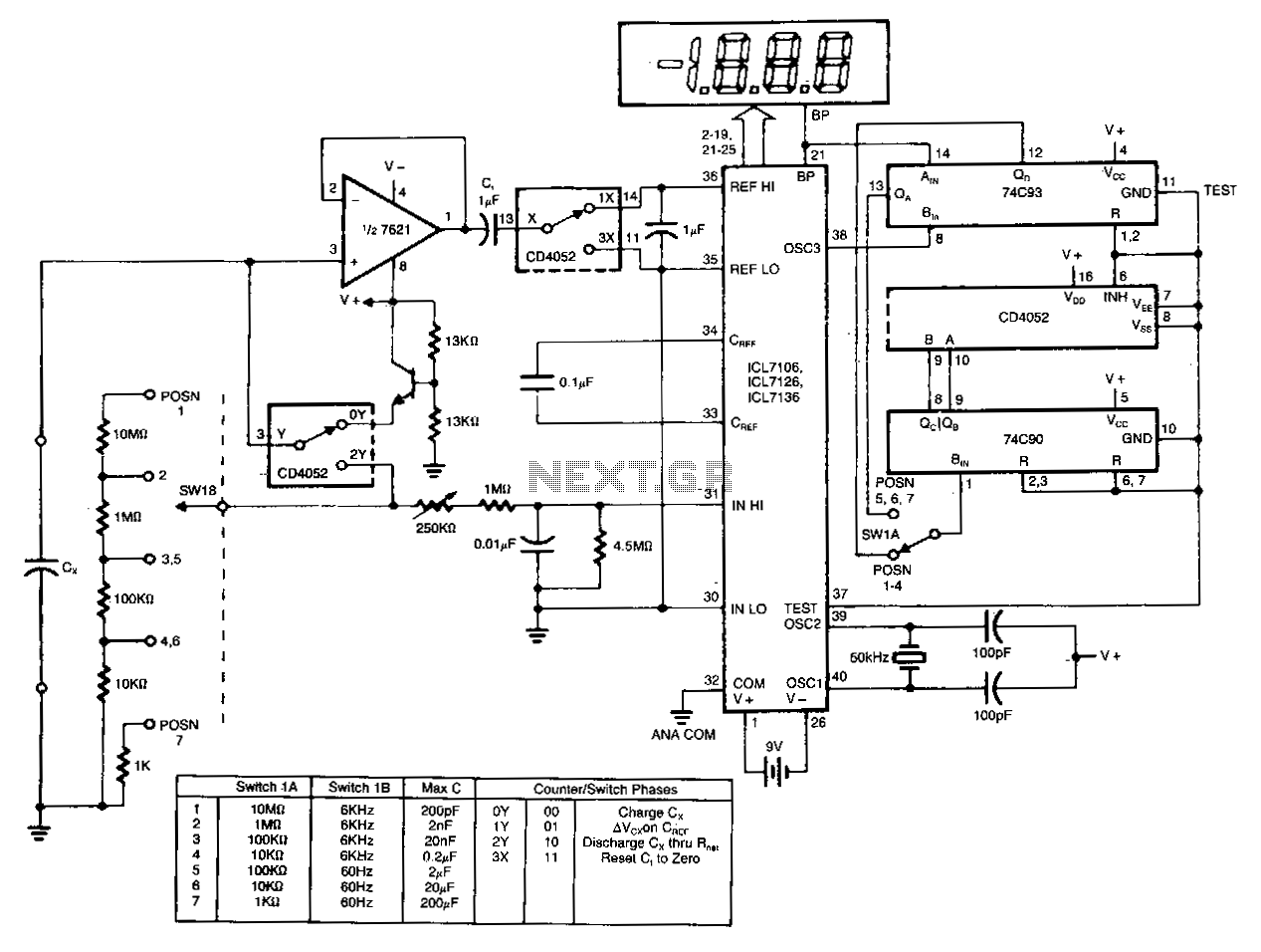
The circuit charges and discharges a capacitor at a crystal-controlled rate and stores the change in voltage achieved on a sample-and-difference amplifier. The current flowing during the discharge cycle is averaged and ratiometrically measured in the analog-to-digital converter (ADC) using the voltage change as a reference. Range switching is accomplished by altering the cycle rate and the current metering resistor. The cycle rate is synchronized with the conversion rate of the ADC by utilizing the externally divided internal oscillator and the internally divided backplane signals. For timing convenience, the switching cycle consists of five counter states, although only four switch configurations are utilized. Capacitances up to 200 pF can be measured, with a resolution down to 0.1 pF in the lowest range. The zero integrator time can initially be set between 1/3 and 112, which represents the minimum auto-zero time. If an optimum adjustment is necessary, the comparator output should be monitored with an oscilloscope under worst-case overload conditions. The output of the delay timer remains low until the comparator exits the rail and enters the linear region, which is typically characterized by significant noise.
The circuit operates by charging and discharging a capacitor at a precise frequency determined by a crystal oscillator, ensuring stable and accurate measurements. The sample-and-difference amplifier captures the voltage variations that occur during the charging and discharging phases, allowing for effective monitoring of the capacitor's behavior. The averaging of the discharge current is critical for obtaining consistent readings, as it mitigates transient fluctuations that could otherwise skew results.
Range switching is a vital feature that enhances the circuit's versatility, enabling it to accommodate a broad spectrum of capacitance values. By adjusting the cycle rate and the resistance of the current metering resistor, the circuit can adapt to different measurement ranges while maintaining accuracy. The synchronization of the cycle rate with the ADC conversion rate ensures that data is collected at optimal intervals, minimizing timing discrepancies that could affect measurement integrity.
The design incorporates a five-state counter for timing the switching cycle, although only four configurations are employed to streamline the operation. This design choice balances complexity and functionality, allowing for efficient capacitor measurement without unnecessary overhead. The capability to measure capacitances up to 200 pF with a resolution of 0.1 pF in the lowest range makes this circuit suitable for precise applications in electronic testing and calibration.
The adjustable zero integrator time is another critical aspect of the circuit, providing flexibility in the auto-zeroing process. Users can set this time based on specific application needs, ensuring that the circuit can accommodate various operational conditions. Monitoring the comparator output with an oscilloscope under extreme conditions allows for fine-tuning, ensuring that the circuit performs optimally even in challenging environments.
Finally, the behavior of the delay timer is essential for ensuring accurate timing of events within the circuit. By remaining low until the comparator transitions out of the rail and into its linear region, the circuit can effectively manage noise and ensure reliable operation. This feature is particularly important in high-precision applications where signal integrity is paramount.The circuit charges and discharges a capacitor at a crystal-controlled rate, and stores on a sample-anddifference amplifier the change in voltage achieved. The current that flows during the discharge cycle is averaged, and ratiometrically measured in the a/d using the voltage change as a reference.
Range switching is done by changing the cycle rate and current metering resistor. The cycle rate is synchronized with the conversion rate of the aid by using the externally divided internal oscillator and the internally divided back plane signals. For convenience in timing, the switching cycle takes 5 counter states, although only four switch configurations are used. Capacitances up to 200 p.F can be measured, and the resolution on the lowest range is down to 0.1 pF.
The zero integrator time can be set initially at 1/3 to 112, the minimum auto-zero time, but if an optimum adjustment is reqnired, look at the comparator output with a scope under worst-case overload conditions. The output of the delay timer should stay low until after the comparator has come off the rail, and is in the linear region (usually fairly noisy).
🔗 External reference
Warning: include(partials/cookie-banner.php): Failed to open stream: Permission denied in /var/www/html/nextgr/view-circuit.php on line 713
Warning: include(): Failed opening 'partials/cookie-banner.php' for inclusion (include_path='.:/usr/share/php') in /var/www/html/nextgr/view-circuit.php on line 713