
Digital Combination LockCircuit Project Tutorial
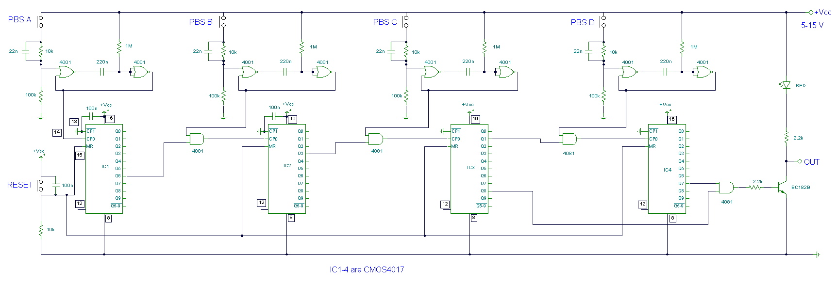
The circuit design features a sequential operation utilizing the CMOS 4017 decade counter, which is designed to count from 0 to 9, with each output pin corresponding to a specific count. The output from the 4017 is connected to an AND gate formed by the CMOS 4081, which requires a specific sequence of button presses to activate the LED indicator.
The debouncing mechanism is critical in this circuit as it ensures that each button press is registered as a single event, preventing multiple counts from a single press due to mechanical bounce. The use of two NOR gates from the CMOS 4001 for each switch effectively filters out noise and provides a clean signal to the counter.
The operation begins with PBS A; only after the correct number of presses is detected will the subsequent PBS B become active. This cascading requirement continues through PBS C and PBS D, creating a multi-step input sequence that must be adhered to in order to activate the output. Specifically, PBS D requires seven presses, followed by PBS C also requiring seven presses, which transitions the output state from 1 to 8.
The AND gate's output is directly linked to an LED, providing a visual indication of successful code entry. The reset functionality is included to allow the user to reset the circuit at any point, ensuring flexibility in operation. The power-on reset feature, enabled by the 100nF capacitor, ensures that the circuit starts in a known state when powered on, preventing any unintended behavior due to residual charge in the circuit components.
Overall, this circuit exemplifies a practical application of digital logic and counting mechanisms, showcasing how various components can interact to create a user-defined output based on a specific input sequence.The circuit above makes use of the CMOS 4017 decade counter IC. Each depression of a switch steps the output through 0 - 9. By coupling the output via an AND gate to the next IC, a predefined code has to be input to create the output. Each PBS switch is debounced by two gates of a CMOS4001 quad 2-input NOR gate. This ensures a clean pulse to the i nput of each CMOS 4017 counter. Only when the correct number of presses at PBS A will allow PBS B to become active. This is similar for PBS C and PBS D. At IC4, PBS D must be pressed 7 times. Then PBS C is again pressed 7 times, stepping from output 1 to output 8. The AND gate formed around CMOS4081 then goes high, lighting the LED. The Reset switch can be pressed at any time. Power on reset is provided by the 100n capacitor near the reset switch. 🔗 External reference
Related Circuits

This digital thermometer circuit diagram utilizes a common 1N4148 diode as the temperature sensor. The diode's temperature coefficient of -2 mV/°C is leveraged to create an accurate electronic thermometer. A digital multimeter is employed to display the measured temperature,...
The circuit is a simple, but accurate Digital Guitar Tuner. It samples the input, which can be directly from the mics of an electric guitar, or from a microphone, if you're using an acoustic guitar. It can of course...
Energia is a rapid prototyping platform for the Texas Instruments MCU Launchpad. It is based on Wiring and Arduino and utilizes the Processing IDE. Energia serves as an accessible development environment for users working with Texas Instruments' microcontroller units (MCUs)...
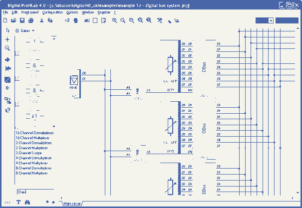
Digital-ProfiLab was designed for measurement and control applications, combining features like circuit and logic simulation, front panel design, and hardware control to one powerful tool. Incoming signals from external devices may be processed and displayed. A circuit editor is...
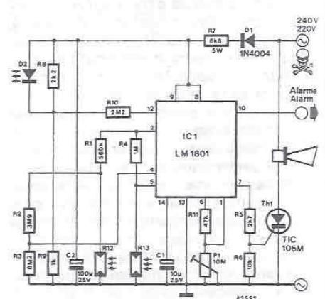
This smoke detector electronic project is designed using the LM1801 and common electronic components. The smoke detector circuit diagram does not utilize ionization detection, gas sensors, or optocouplers; instead, it employs two photoresistors (LDRs) and an LED. The circuit...
The circuit of the Witnesscam consists of four integrated circuits and a few passive components, making it quite simple. The AVR ATmega32 microcontroller plays a crucial role in the design. By incorporating a JPG camera module, a PIR sensor,...