Digital-frequency-doubler

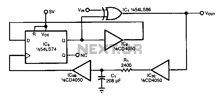
The circuit doubles the frequency of a digital signal by operating on both signal edges. Each transition causes the exclusive-OR gate IC1 to produce a pulse, which clocks flip-flop IC3 after propagating through buffers IC2C and IC2B. If capacitor C1 is removed, the circuit produces narrow output pulses. By including C1, a desired duty cycle for a given input frequency fin can be obtained.
The described circuit utilizes a frequency-doubling technique by leveraging both the rising and falling edges of the input digital signal. The core component of this circuit is the exclusive-OR gate, designated as IC1. This gate is responsible for detecting transitions in the input signal. Each transition detected by IC1 generates a pulse that is sent to a flip-flop, represented as IC3. The flip-flop serves as a storage element that synchronizes the output signal with the clock pulses received from IC1.
To ensure the proper timing and signal integrity, the circuit incorporates two buffer stages, labeled IC2B and IC2C. These buffers are crucial for isolating the IC1 output from the flip-flop input, thereby preventing loading effects that could distort the signal. The buffers also help to maintain the signal's integrity as it propagates through the circuit.
The inclusion of capacitor C1 plays a significant role in shaping the output signal. When C1 is connected, it influences the timing characteristics of the output pulses, allowing for the adjustment of the duty cycle. The duty cycle is the ratio of the time the output signal is high to the total period of the signal. By carefully selecting the capacitance value of C1, the circuit can be fine-tuned to achieve the desired duty cycle for a specific input frequency (fin). Conversely, if C1 is removed, the circuit will produce narrow output pulses, which may not be suitable for applications requiring a specific duty cycle.
Overall, this circuit design is effective for applications that require frequency doubling while maintaining control over the output pulse characteristics. Adjustments to the capacitor provide flexibility in tailoring the output to meet specific requirements.The circuit doubles tbe frequency of a digital signal by operating on botb signal edges. Each transition causes exclusive-OR gate IC1 to produce a pulse, which clocks flip-flop IC3 after propagating through buffers IC2C and IC2B. Ifyou remove capacitor Cl, tbe circuit produces narrow output pulses. By including Cl, you can obtain a desired duty cycle for a given input frequency fin.