
Electronic-time-delay
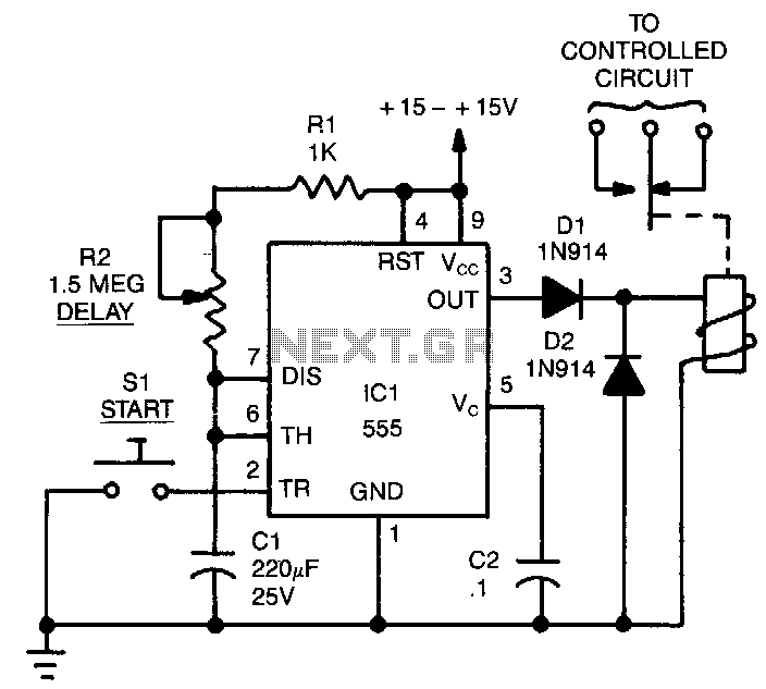
The time delay, T, in seconds is calculated using the formula: T = 1.1 x C1 x (R1 + R2). The resistances are measured in megohms and the capacitances in microfarads. The combined resistance of R1 and R2 should be no less than 1000 ohms and no greater than 20 megaohms. Pressing switch S1 initiates the timing cycle. An alternative method to start the timing cycle is by applying a low-going pulse instead of using S1. With the specified values and considering the tolerances of the 200 µF capacitor, the delay will range from 4 minutes and 50 seconds to 7 minutes and 26 seconds. The output terminal, pin 3, of the 555 timer is typically low and transitions to high during the timing cycle. This output can either sink or source currents up to 200 mA, allowing connection of a load such as a relay coil between pin 3 and Vcc or between pin 3 and ground, based on circuit requirements. When the relay is connected between pin 3 and ground, it remains de-energized except during the timing cycle, which conserves power and allows the integrated circuit (IC) to operate at a lower temperature.
The circuit utilizes a 555 timer configured in monostable mode, where the timing cycle is initiated by pressing switch S1 or by a low-going pulse. The time delay is determined by the values of the capacitor C1 and the resistors R1 and R2, with the formula T = 1.1 x C1 x (R1 + R2) ensuring that the timing is accurate within the specified ranges. The resistors R1 and R2 are crucial for setting the timing duration; therefore, they must be selected carefully to comply with the requirement that their sum lies between 1000 ohms and 20 megaohms.
During the timing cycle, pin 3 of the 555 timer outputs a high signal, which can be utilized to drive a relay. The relay can be connected in two configurations: one that connects the relay coil to Vcc when pin 3 goes high, or another that connects it to ground. The configuration that connects the relay to ground is preferred in applications where power efficiency is critical, as it keeps the relay de-energized most of the time, activating only during the timing period. This approach minimizes heat generation in the IC and enhances the longevity of the components involved.
In summary, this circuit design effectively integrates timing control with relay actuation, leveraging the versatile capabilities of the 555 timer while adhering to specified electrical parameters to ensure reliable operation.The time delay, T, in seconds is: T = 1.1 x Cl x (Rl + R2). The resistances are in megohms and capacitances in microfarads. The sum of R1 and R2 should not be Jess than 1000 0 nor higher than 20 MO. Pressing S1 starts the timing cycle. A low-going pulse, instead of S1 can also be used to initiate the timing cycle. With the values shown and allowing for the tolerances of the 200-JtF capacitor, the delay will range from 4 minutes and 50 seconds to 7 minutes and 26 seconds. The output terminal, pin 3, of 555, is normally low and switches high during the timing cycle. The output can either sink or source currents up to 200 mA. Therefore, a load such as a relay coil can be connected between pin 3 and Vccc or between pin 3 and ground, depending on circuit requirements. When the relay is connected between pin 3 and ground, it is normally de-energized so it is energized only during the timing cycle.
Connecting the relay to ground will. save power and allow the IC to run cool. 🔗 External reference