
Extensible Multiple Device Programmer 1
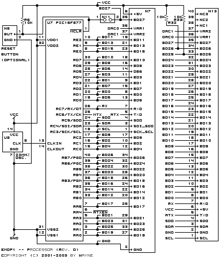
The circuit functions as a robust power management and communication system, integrating various voltage regulation stages to ensure stable operation across different components. The initial 24VDC input is effectively managed through a series of regulators, ensuring that downstream devices receive the appropriate voltage levels for optimal performance. The use of the MAX232 and RS-422 transceivers allows for flexible communication options, accommodating different signaling standards while maintaining compatibility with established protocols. Additionally, the inclusion of biasing resistors and termination resistors enhances signal integrity, particularly in RS-422 applications.
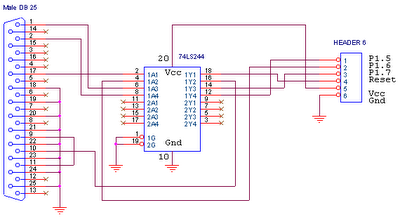
The microcontroller, a central component of this design, is programmed to manage both analog and digital signals, with the I2C interface facilitating communication with the D/A converter. The conversion process is crucial for applications requiring precise analog outputs, and the design includes provisions for signal conditioning through operational amplifiers to achieve the desired voltage swing. Overall, the schematic represents a well-thought-out integration of power supply management, communication interfaces, and signal processing, making it suitable for a range of electronic applications.The power supply takes its power from a 24-volt VDC wall wart either via N1, an on board connector, or via N10 an off-board connector. The power switch is either mounted on board or off-board via connector N2. The fuse can either be on board at F1 or off board via connector N3. Diode D1 is a shorting diode that should short the supply and burn out the fuse if the power supply gets hooked up backwards. The 24VDC is regulated to 24 volts via C1, U1, and C2. The 24Volts is regulated down to 15 volts via U2 and C3. The 15 volts is regulated down to 5 volts vis U3 and C4. N is available if people wish to provide an source of power supply voltages and leave U1-U3 empty. The EMDP1 can communicate with its host processor via either RS-232 or RS-422 signaling. The RS-232 signaling takes place via an industrys standard female DB9 connector. The RS-422 signaling done via an RJ45 connector using standard Cat5 (catagory 5) cabling. The RS-422 is wired to conform to my SimpliciNet `standard`, which allows both RS-422 signalling and power over the same cable. The RS-232 signals are converted to logic levels using U3, a standard MAX232 level convert chip. U4 is an RS-422 transceiver configured as an RS-422 transmitter and U5 is an RS-422 transceiver configured as a receiver.
Resister R7 is 100 ohms of RS-422 termination and R8 and R9 provide biasing resistors to ensure that a logic high level is output if now RS-422 signal is present. U6A is takes the logical or of the received signals from the RS-232 and RS-422 and sends them on to the microcontroller serial receive line.
U6B logically or`s the transmit signals from the adaptor (via U11A) or from the microcontroller (MTX). R27 is forces the adaptor signal out if the microcontroller chip is being programmed by the bootstrap adaptor.
The U7 microcontroller is a Microchp ® PIC16F877. U8 is a 20MHz crystal oscillator chip to provide the required clock signal. Connector N8 and resistor R6 is an optional reset button circuit. Jumper N11 shorted when the bootstrap adaptor is being used to program the microcontroller. Connector N7 is a 40-pin connector that is connected to a 37-pin D connector. In addition, the exact same signals are routed to N13 of the `universal` plug. The microcontroller controls the digital to U10 analog converter using standard I2C signalling. The D/Aconverter is a MAX518. (I`m quite nervious about the continued availabilty of this chip; most I2C chips are being manufactured in surface mount packages only. ) Resistors R28 and R29 are the required pull-up resistors for I2C. The outputs of the MAX518 is run into two op amps in U9 configured as linear amplifiers to take the 0 to 5 volt output swing of the D/A and convert it 0 to 24 volt swing.
The capacitors C12 and C13 prevent overshoot. Connector N12 is used by the bootstrap adaptor to get 24 volts of power to feed back to the microcontroller at 13 volts for programming purposes. 🔗 External reference
Related Circuits
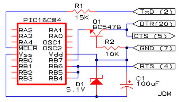
Affordable PIC Programmer. This programmer is compatible solely with the PIC16F84 microcontroller. It is reliable, as it rarely encounters errors, and functions well with nearly all computer systems, in contrast to some alternatives. The PIC programmer designed for the PIC16F84...
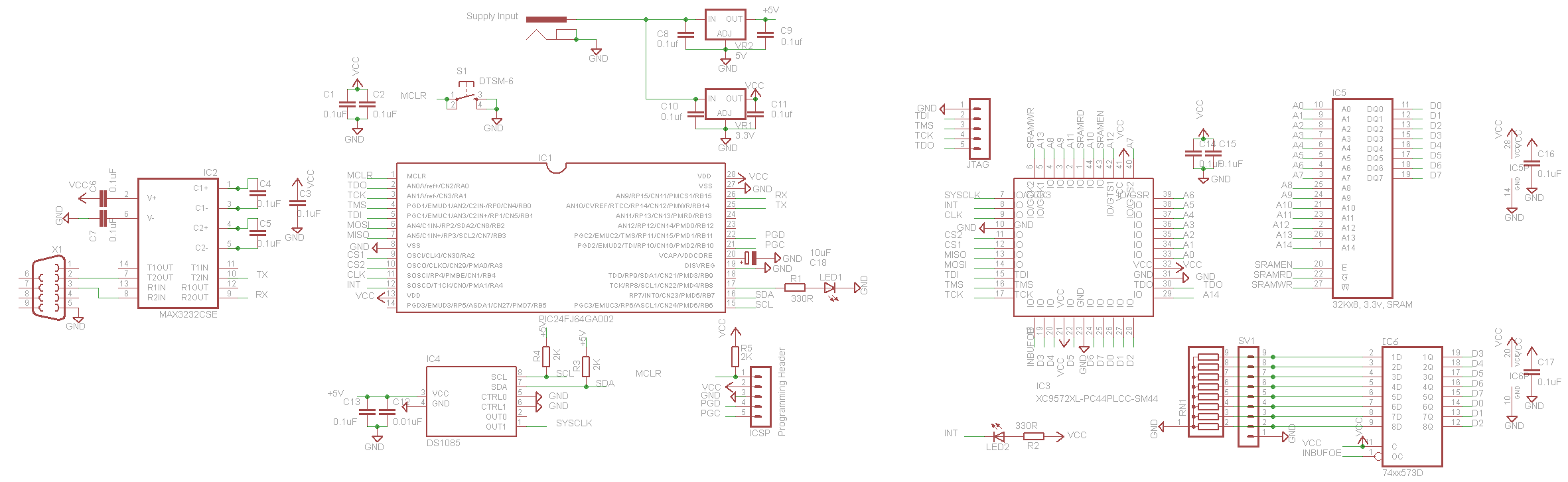
Complex programmable logic devices (CPLDs) contain the building blocks for hundreds of 7400-series logic ICs. Complete circuits can be designed on a PC and then uploaded to a CPLD for instant implementation. CPLDs are integrated circuits that provide a versatile...
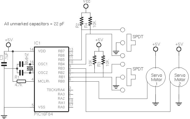
A modified version of the previous program allows control of multiple servomotors, utilizing all available I/O lines on port B. The following listing demonstrates the control of two servos similarly to how a single servo was managed in the...

This design circuit is for a stereo encoder utilizing the BH1417 Stereo Encoder IC. The circuit incorporates pre-emphasis and a limiter to ensure consistent audio levels during transmission. A low-pass filter is included to block audio signals above 15...
This circuit is designed for use with ATMEL Microcontroller ICs, specifically the AT89Sxx and ATMEGA series. It operates using the MISO, MOSI, SCK, and RESET signals. This circuit serves as a foundational interface for programming and communication with ATMEL microcontrollers,...
As the demand for VRM output current increases, the components and parts of the SR-Buck converter can no longer meet the requirements for the new generation microprocessors needing 100 A. Additionally, creating filtering inductance for high currents is quite...