
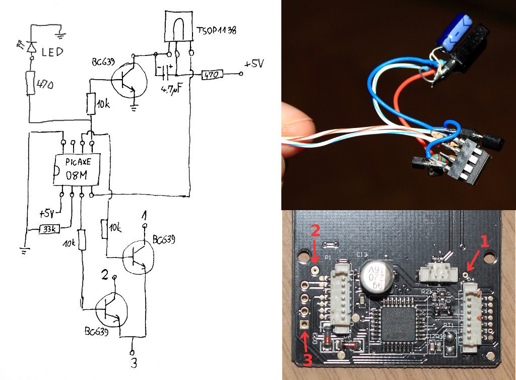
Flash Trigger

The circuit design utilizes a single transistor amplifier as the core component, which serves to amplify the signal from the piezo drum. This configuration is critical for ensuring that the trigger is responsive to the mechanical vibrations generated by the drum. The SCR (Silicon Controlled Rectifier) is integrated to control the power delivered to the flashes, allowing for precise triggering. The Mark II version enhances the initial design by incorporating a delay and debounce mechanism, which is essential for preventing false triggering caused by noise or vibrations.
The vero-board layout is optimized for compactness, ensuring that the components are arranged to minimize signal path lengths and reduce potential interference. The inclusion of the Zobel network (C5/R2) serves to stabilize the amplifier and filter out high-frequency noise, thereby improving the overall performance of the trigger circuit. The use of miniature linear potentiometers allows for fine adjustments to be made, catering to specific user needs. The choice of a Jiffy-type box for housing the circuit not only protects the components but also enhances portability and ease of use.
In terms of output, the design allows for flexibility, enabling connections to various triggering mechanisms. The recommendation to use the lowest power setting on flashes is crucial, as this setting ensures a minimal flash duration, which is vital for capturing high-speed events without motion blur. The testing phase on a breadboard is an essential step, allowing for troubleshooting and adjustments before final assembly. This approach ensures that the circuit functions reliably and meets the intended application requirements. Overall, the design is a robust solution for those looking to create a reliable high-speed photography trigger system.The following is a (hopefully clear) description of the final version of the trigger used and a circuit diagram for anyone wishing to construct their own. So bear with me while I fumble out some words The initial version of this trigger was a very simple single transistor amplifier, a piezo drum and an SCR.
It performed well for quite a while but the need to drive the flashes directly (rather than from eBay radio triggers) and to have a system of delay and debounce led me to constructing a Mark II. I also did a more permanent job of the circuit by vero-boarding and casing it. There are a few circuits like this out there on the net but overall I found the quality of the designs quite poor some almost like they had never actually been built.
So I aggregated a few of the designs, added some of my own stuff and came up with this. Rest assured that if you build this correctly it will work as I have a completed one myself. It is a little over engineered and several components could possibly be discarded but I desiged it with best practices in mind and following all the guidelines in the ICs datasheets. In the BOM I have indicated Jaycar part numbers for the various non R/C components. However the parts are quite common and I am sure they all can be sourced from any decent supplier or from Digikey/Farnell.
Pictures of my own implementation follow to give an idea of how you might case the circuit. The case I used is a simple Jiffy type box which has the advantage of a battery compartment for the 9V cell required to power the circuit. Makes for a nice clean unit. The pots are miniature types and linear. Finer tuning in the low end could be achieved if they were logarithmic I guess it depends on your requirements as to weather that would be useful.
This is the circuit on veroboard inside the case. The C5/R2 Zorbel network are the only components not visible as they are on the back of the board having being added as an afterthought. The wires visible run to the pots, switches and connectors. The red tape insulates the circuit from the switch terminals which could potentially touch the board due to their depth.
And finally all squared away and labelled. For output you can either get some cheap eBay 3. 5mm to PC Sync cables (or make your own) or run one of the outputs into a radio trigger transmitter. Though the later presents some problems for high speed photography see post and comments here. However the flashes are connected they must be used in their LOWEST power setting. This ensures the minimum flash period which is essential for high speed. Both Canon and Nikon flashes are capable of producing approx 1/30000s bursts on their lowest setting. If you are going to have a shot at building it I would recommend initially doing it on a breadboard. Get the amp working first you can substitute the R3 resistor with a speaker and see if the mic is being reasonably amplified.
Keep in mind this is not a high end audio amplifier! As long a there is no oscillating/reverberating or high levels of distortion you are probably good to go. I used a old PC speaker to test with. After you get the amp going reliably (which has the most potential to cause trouble being analog) proceed to the delay/debounce which is mostly logic.
When building the amp try to keep it as compact as possible long tracks and cables are never an amps best friend. 🔗 External reference
Related Circuits
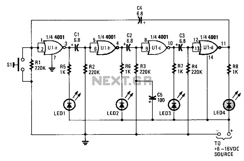
When power is initially applied, two of the LEDs illuminate while the other two remain off until the timing cycle reverses. The LEDs flash in pairs; however, by pressing and holding switch S1 until only one LED is lit,...
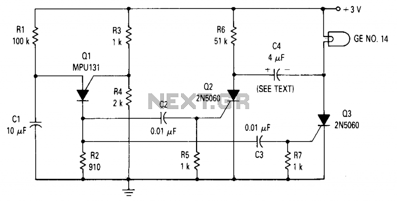
The circuit consists of a relaxation oscillator created by Q1 and an SCR flip-flop formed by Q2 and Q3. When the supply voltage is applied to the circuit, the timing capacitor C1 charges to the firing point of the...

There have described the involvement benefited LM3909 circuit, which is quite expensive. That's why I prefer to use a much cheaper known timer 555th. Involvement of the tree is a very simple scheme is to figure 2. It is...
The YN-460 is an affordable manual-only shoe mount flash produced by the Chinese company Yongnuo. It has gained popularity within the strobist community primarily due to its low price and satisfactory performance. To adjust the flash power level, users...
The concept of this economical flashing LED indicator is straightforward. It employs a low-frequency oscillator to drive two LEDs connected in anti-parallel. In the circuit diagram, it can be observed that the current flows for a brief duration with...
High-energy capacitors can produce hundreds of amps when short-circuited, potentially causing severe burns, fires, and property damage. It is essential to be aware of these hazards when using such capacitors and to take precautions to avoid accidental short-circuits. The...