
Flip-Flop Timer Using 4017
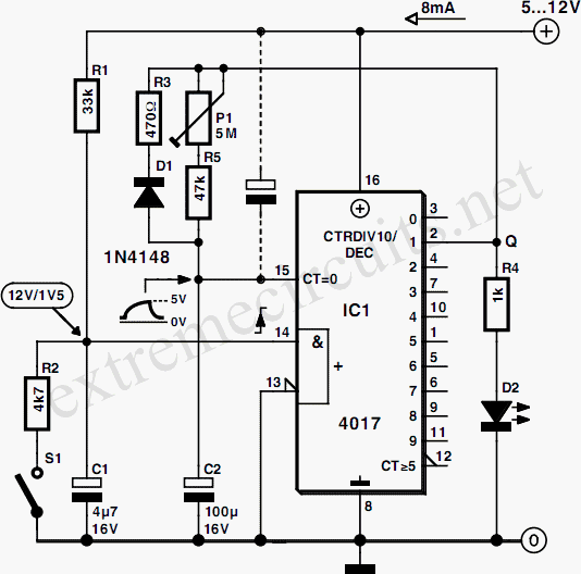
The circuit utilizes the 4017 CMOS decade counter, which is a versatile component often employed in timing and counting applications. The operation begins with the press of switch S1, which initiates the discharge of capacitor C1 through resistor R2. This action sets the stage for a clock pulse to be generated when S1 is released, allowing C1 to charge through R1, thereby creating a rising edge at the clock input of the IC.
The output Q1 of the 4017 will transition high, activating the LED D2 via resistor R4. The simultaneous charging of capacitor C2 through preset resistor P1 and resistor R6 is crucial, as it sets the timing interval for the circuit. The design allows for an adjustable timing range, which can be fine-tuned by varying the value of P1. The timing mechanism is based on the voltage threshold of C2, where reaching approximately half the supply voltage triggers a reset of the IC.
Upon reset, the output Q1 goes low, turning off LED D2, and capacitor C2 discharges through diode D1 and resistor R3, returning the circuit to its initial stable state. This cycle continues with the pressing of S1, providing a simple yet effective timer functionality.
The current consumption characteristics of the circuit are noteworthy, as it operates at minimal power in the reset state, making it suitable for battery-powered applications. The increase in current draw during the active state is primarily due to the LED, which serves as a visual indicator of the timer's operation.
It is also important to consider the alternative configuration for capacitor C2, which connects it to the supply rail. This modification ensures that the IC starts in a reset state upon power-up, mitigating any issues related to indeterminate states. However, this approach introduces the potential for noise from the supply rail to influence the reset pin, which may inadvertently affect the timing accuracy of the circuit. Thus, careful consideration of the circuit's environment and power supply stability is essential for optimal performance.This circuit shows how a 4017 CMOS decade counter can be used to build a timer circuit. Push-button S1 will discharge capacitor C1 through resistor R2. When S1 is released, C1 will charge up through R1 causing a rising edge at the clock input of IC1. This causes the output Q1 to go high (to the supply voltage). Current will‚ow through R4 and LE D D2 will light. At the same time C2 will begin charging through preset P1 and R6. When the voltage on C2 reaches approximately half the supply voltage it will reset IC1. Q1 will go low, the LED will go off and C2 will discharge through D1 and R3. The circuit will now remain stable in this reset condition until S1 is pressed again. Preset P1 allows the ON time of the circuit to be adjusted between 5 seconds and 7 minutes. The current consumption of this circuit in its reset state is only a few micro-amps, rising to approximately 8mA mainly due to the LED current, when S1 is pressed. When power is applied to the circuit IC1, can be in an indeterminate state and the LED may be on. Pressing S1 until the LED goes off clears this condition. Alternatively C2 may be connected to the supply rail (as shown dotted in the diagram) this will ensure that IC1 will always power up in a reset state.
A disadvantage of this conguration is that any noise on the supply rail will be coupled through to the reset pin of IC1 and may affect the timing period. 🔗 External reference
Related Circuits
The circuit diagram is designed to control audio tone. This circuit utilizes the TDA 1524 tone control integrated circuit (IC), which encompasses controls for balance, bass, treble, and volume within a single component. A potentiometer is employed in series...
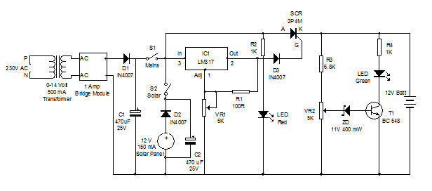
Battery charger utilizing solar and electrical power with a circuit diagram. This dual power source battery charger can charge a lead-acid battery using two different power sources. The battery charger circuit is designed to efficiently charge a lead-acid battery by...
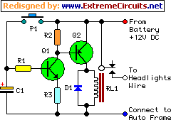
This device is a simple timer that keeps the headlights of a vehicle on for approximately 1 minute and 30 seconds, allowing for illumination when accessing dark areas without the need to return to switch off the lights. Pressing...
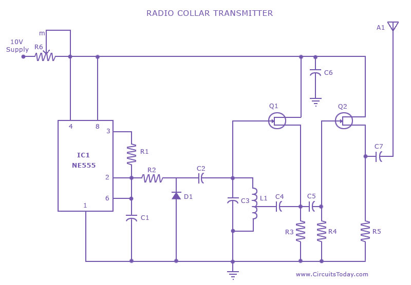
This is a radio transmitter circuit diagram designed for integration into radio collars using the NE 555 integrated circuit. The circuit transmits a pulse in the FM band, specifically between 88 MHz and 105 MHz. The radio transmitter circuit utilizes...
The CDCF5801 provides clock multiplication from a reference clock (REFCLK) signal with the unique capability to delay or advance the CLKOUT/CLKOUTB with steps of only 1.3 mUI through a phase aligner. For every rising edge on the DLYCTRL pin,...
This circuit illustrates a remote control system utilizing a radio telephone circuit diagram. Features include the ability to switch appliances from any distance, overcoming various limitations. The remote control circuit employs radio frequency (RF) technology to facilitate wireless communication between...
Warning: include(partials/cookie-banner.php): Failed to open stream: Permission denied in /var/www/html/nextgr/view-circuit.php on line 713
Warning: include(): Failed opening 'partials/cookie-banner.php' for inclusion (include_path='.:/usr/share/php') in /var/www/html/nextgr/view-circuit.php on line 713