
Flyback Power Supply Powers Subscriber Line Interface Circuit

The design of the power supply circuit for the SLIC in cable and xDSL modems is critical to ensure reliable operation and compatibility with existing telephone systems. The SLIC's ability to handle both ringing and conversation states necessitates careful consideration of the voltage and current requirements. The flyback topology utilized in the design allows for efficient voltage conversion and regulation, essential for maintaining the necessary output levels under varying load conditions.
The use of an n-channel MOSFET in this circuit is advantageous due to its low on-resistance, which reduces conduction losses during operation. This is particularly important in applications where high efficiency is required, such as in telecommunications equipment that must operate continuously without overheating. The control IC's ability to switch between current-mode and voltage-mode control further enhances the performance of the power supply, allowing for dynamic adjustments based on the load conditions.
Additionally, the multi-winding transformer design supports the simultaneous generation of both the 24-V and 72-V outputs, facilitating a compact and efficient solution. This design choice also aids in achieving good cross-regulation, ensuring that fluctuations in one output do not adversely affect the other. The operational amplifier's role in generating error signals is crucial for maintaining the desired output voltage levels, despite variations in load and input conditions.
In summary, the power supply circuit for the SLIC in cable and xDSL modems exemplifies a well-engineered solution that meets the demanding requirements of modern telecommunications. Its design considerations, including efficiency, voltage regulation, and load handling, contribute to the overall reliability and performance of the modem, ensuring that it can effectively interface with existing telephone infrastructure while providing high-quality service to subscribers.Cable and xDSL modems are experiencing increasing popularity. For this reason, many designs are now required to interface with existing telephones at the subscriber`s location. The subscriber line interface circuit (SLIC) within the modem has the additional burden of ringing the phone as well as providing loop current while a conversation is takin
g place. While the phone is ringing and "on-hook, " it appears as an 8k resistance in series with another 1k of capacitive reactance. Typically, the SLIC must be capable of driving this impedance with a 45-VRMS, 20-Hz sinewave with a negative dc-offset in order to ring the phone.
Therefore, a high voltage of between ’50 and ’105 V is usually mandated by the SLIC. Once the handset is lifted, the phone places a much lower impedance across the phone terminals, and the SLIC goes into a 20-mA constant-current mode. As a result, the SLIC only needs a power supply of ’24 V. Figure 1 shows the schematic of the power supply for the SLIC portion of the modem. This circuit provides multiple outputs from a single power switch and control IC. It also uses an efficient n-channel MOSFET with low voltage stress. A low input voltage powers a flyback topology. The input source could be either a widely differentiating (generally 2. 5 to 1) output from an ac adapter, or a regulated supply used by some other portion of the system. U2 is the brain of the power supply, as it modulates Q2`s duty factor to control the output voltage. Also, it produces a reference voltage inverting amplifier U1 uses to generate an error signal. The control IC can perform either in current-mode or voltage-mode control. A key advantage of the multi-winding approach is that a single control circuit and single MOSFET can supply two telephony voltages.
Good cross-regulation can be achieved even though the SLIC places large current swings on both outputs ( Fig. 2 ). With the ’24-V output, variations range from 3 mA of load current (when all phones are idle) to 80 to 100 mA of current (when all phones are off-hook).
The ’72-V output current can vary from 1 mA to a peak of 100 mA. Changes in the ’24-V output voltage occur due to the operational amplifier`s offset voltages, which are typically 3%, as well as divider and reference tolerances. Capable of such tolerances, the ’72-V output also offers cross regulation of the transformer and the fluctuating diode voltage drops.
Even with all of these variables, however, the ’72-V output`s worst-case variation is less than 4 V, way below the 14-V requirement. Because of its low conduction and switching losses, the n-MOSFET, multi-output flyback configuration provides excellent efficiency.
The efficiency measurements with the ’72-V output loaded to full current are given over a wide input voltage range ( Fig. 3 ). This design has been optimized with approximately 90% efficiency for a 12-V input. For the low input voltages, the efficiency is somewhat lower due to the increased conduction losses in the MOSFET.
But at high voltages, the higher switching losses cause the lower efficiency. 🔗 External reference
Related Circuits
Typical segment display LEDs consume around 25 mA for each segment and should be limited to this current with resistors. For a six-digit display to be current limited, at least 42 series resistors are needed. The brightness of the...
Every electronic device primarily requires a DC power supply for operation. This is a fundamental requirement for any construction project. Consequently, there is a need to obtain multiple voltage values for cost efficiency, convenience, and compact arrangement in various...
Circuits C1, R1, varistors, L1, and R2 form a filter circuit that includes a primary power supply capable of filtering out transient overvoltage inputs. The circuit also consists of C2 and R2, with additional components C3, C4, and L2....
Photovoltaic (PV) technology involves the application of solar cells to convert sunlight directly into electricity. The provided manual on Photovoltaic Power Systems outlines practices in accordance with the 2005 National Electrical Code (NEC) relevant to PV power systems. This...
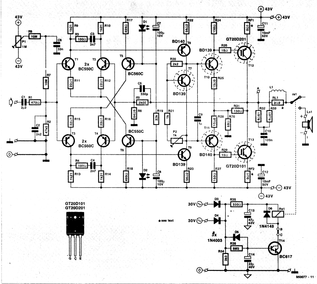
The power amplifier Hi-Fi OCL 120W RMS is designed to operate effectively when paired with a suitable power supply circuit and 8-ohm speakers. This circuit exclusively utilizes transistors without any integrated circuits, resulting in a clean sound output. The...
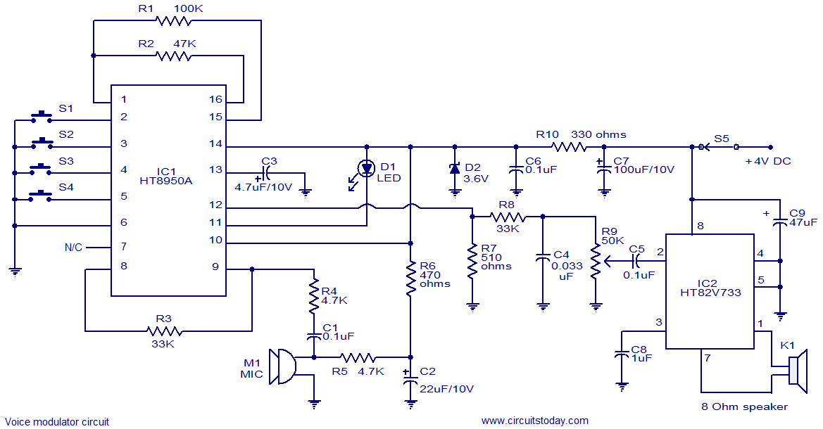
This is a versatile voice modulator circuit utilizing the HT8950A IC from Holtek Semiconductors. The IC can generate seven upward or downward frequency steps based on the input voice at a rate of 8 Hz. Additionally, it features two...
Warning: include(partials/cookie-banner.php): Failed to open stream: Permission denied in /var/www/html/nextgr/view-circuit.php on line 713
Warning: include(): Failed opening 'partials/cookie-banner.php' for inclusion (include_path='.:/usr/share/php') in /var/www/html/nextgr/view-circuit.php on line 713