
Four-output-waveform-generator
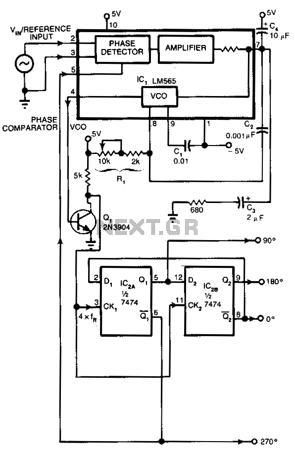
Many applications require control signals that have phase shifts relative to an input signal. This circuit accepts a sine, square, or triangular wave as an input reference signal and produces square-wave outputs with 0°, 90°, 180°, and 270° phase shifts concerning the input. The circuit features two integrated circuits (ICs): an LM565 phase-locked loop and a 7474 dual-D positive edge-triggered flip-flop. Resistor R1 and capacitor C1 are used to set the free-running frequency of the LM565's voltage-controlled oscillator (VCO). R1 should be adjusted so that the frequency is approximately four times that of the input reference signal. The LM565 responds to input signals greater than 10 mV peak-to-peak, with 3 V peak-to-peak being the maximum allowable input level for the chip. Transistor Q1 matches the LM565's output to the flip-flops' inputs. The outputs of the flip-flops provide TTL-compatible square-wave signals with 0°, 90°, 180°, and 270° phase shifts relative to the input signal.
The circuit employs the LM565 phase-locked loop (PLL) as the core component for generating phase-shifted signals. The LM565 operates by locking onto the frequency of the input signal and then producing a corresponding output frequency that is adjustable based on external components. The VCO within the LM565 is configured using R1 and C1, where the values of these components determine the oscillation frequency. It is critical to set R1 to achieve a frequency that is four times that of the incoming reference signal to ensure proper phase shifting.
The 7474 dual-D flip-flop is utilized to generate the desired phase shifts. Each output of the flip-flop corresponds to a specific phase shift: the first output provides the original signal (0°), the second output provides a 90° phase shift, the third output delivers a 180° phase shift, and the fourth output yields a 270° phase shift. This arrangement allows for versatile control in applications that require precise timing and phase relationships between signals.
The transistor Q1 serves as a buffer, ensuring that the output from the LM565 is compatible with the input requirements of the 7474 flip-flops. This buffering is essential for maintaining signal integrity and preventing loading effects that could distort the output signals. The overall design is robust, accommodating a range of input signal types and producing reliable TTL-compatible outputs that can be easily interfaced with other digital circuitry. The circuit is suitable for various applications, including signal processing, communication systems, and timing applications where phase relationships are crucial.Many applications require control signals that have phase shifts with reference to an input signal. Circuit accepts a sine, square, or triangular wave as an input reference signal and produces square-wave outputs with 0", 90", 180", and 270" phase shifts with respect to the input. Figure 38-3B shows the input and output waveforms. The circuit contains two !Cs: an LM565 phase-locked loop and a 7474 dual-D positive edge-triggered flip-flop.
R1 and C1 set the free-running frequency of the LM565"s VCO. You should adjust R1 so that the frequency is approximately four times that of the input reference signal. The LM565 responds to input signals greater than 10 mV pk-pk; 3 V pk-pk is the chip"s maximum allowable input level. Q1 matches the LM565"s output to the flip-flops" inputs. The flip-flops" outputs provide the TTL-compatible square-wave signals with 0", 90", 180", and 270" phase shift with reference to the input signal.
🔗 External reference
Warning: include(partials/cookie-banner.php): Failed to open stream: Permission denied in /var/www/html/nextgr/view-circuit.php on line 713
Warning: include(): Failed opening 'partials/cookie-banner.php' for inclusion (include_path='.:/usr/share/php') in /var/www/html/nextgr/view-circuit.php on line 713