
Frequency Shift Keying (FSK) Demodulator
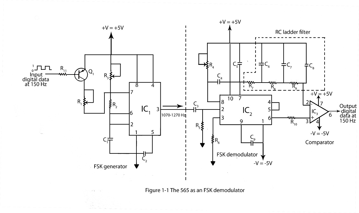
The frequency shift keying (FSK) technique is a form of digital modulation where the frequency of a carrier signal is varied in accordance with the binary data being transmitted. This method is particularly effective in environments with noise, as it allows for robust signal detection. The FSK demodulator circuit typically consists of a frequency discriminator, which translates the frequency variations back into the original binary data.
In this specific implementation, the 565 integrated circuit (IC) is employed as the core component of the FSK demodulator. The 565 IC is a phase-locked loop (PLL) that can be configured to detect frequency shifts effectively. It operates by locking onto the frequency of the incoming signal and producing an output that corresponds to the frequency changes, which represent the binary data.
The circuit diagram of the FSK demodulator includes the following key components:
1. **Input Signal**: The modulated FSK signal is fed into the circuit, typically through a capacitor for AC coupling.
2. **565 IC Configuration**: The 565 IC is configured in a manner that allows it to detect the two distinct frequencies used in the FSK modulation. External resistors and capacitors are connected to the IC to set the appropriate bandwidth and response time.
3. **Output Stage**: The output from the 565 is a square wave signal that corresponds to the original binary data. This output can be further processed or fed into a microcontroller for digital processing.
4. **Power Supply**: The circuit requires a stable power supply, typically in the range of 5V to 15V, depending on the specifications of the 565 IC.
5. **Filtering and Smoothing**: Additional filtering components may be included to smooth out any noise or fluctuations in the output signal, ensuring a clean representation of the binary data.
Overall, the circuit diagram and configuration of the FSK demodulator using the 565 IC provide a reliable and efficient method for demodulating frequency-shifted signals, making it suitable for various communication applications. Proper layout and component selection are crucial for achieving optimal performance and signal integrity in the final design.Frequency shifting keying technique is used to transmit binary data. The circuit diagram with description fsk demodulator used 565 IC for frequency shift keying. 🔗 External reference
Related Circuits
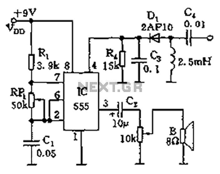
The circuit features a 555 timer integrated circuit along with components R1, RP1, C1, and others, which together form an audio oscillator. The frequency of the oscillator is determined by the formula f = 1.44 / ((R1 + 2...
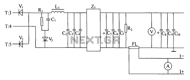
Alternating positive and negative voltage pulses from the secondary winding of a high-frequency transformer (T) are full-wave rectified by high-frequency switching diodes (V1, V2). The output is then filtered through inductors (L1) and capacitors (C2, C3, C4) which form...
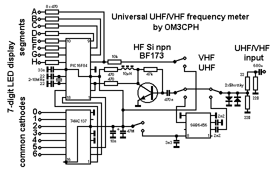
Having found a u664b prescaler chip (Telefunken) from an old TV tuner, I decided to build a valid frequency counter using PIC16F84. The prescaler I use is able to divide by 64 every frequency from 30 to 1300 MHz....
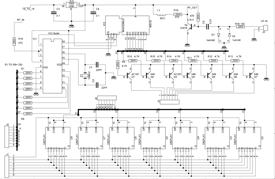
This is a simple frequency counter based on the microcontroller PIC16F84. Its maximum operating frequency is approximately 30 MHz, with a resolution of 10 Hz and low current consumption of 15 mA. The assembly process is straightforward. The device...
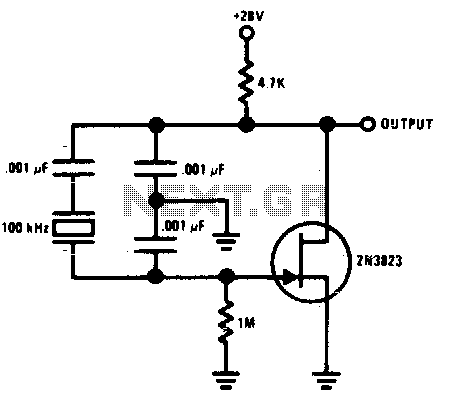
This Colpitts crystal oscillator is ideal for low-frequency crystal oscillator circuits. Excellent stability is assured because the 2N3823 JFET circuit loading does not vary with temperature. The Colpitts crystal oscillator is a type of electronic oscillator that utilizes a combination...
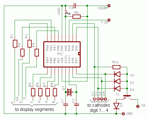
This document outlines the construction of a compact frequency counter utilizing an inexpensive PIC microcontroller and several seven-segment LED displays. A PIC programmer necessary for programming the PIC 16F628 is accessible on DL4YHF's website. Requests for programmed PICs or...
Warning: include(partials/cookie-banner.php): Failed to open stream: Permission denied in /var/www/html/nextgr/view-circuit.php on line 713
Warning: include(): Failed opening 'partials/cookie-banner.php' for inclusion (include_path='.:/usr/share/php') in /var/www/html/nextgr/view-circuit.php on line 713