Frequency Synthesizers
1. Definition and Purpose of Frequency Synthesizers
Definition and Purpose of Frequency Synthesizers
A frequency synthesizer is an electronic system that generates a range of frequencies from a single, stable reference oscillator. These synthesized frequencies are phase-locked to the reference, ensuring high spectral purity and precise control. The core function is to provide programmable output frequencies with low phase noise, minimal spurious signals, and fast switching times—critical for applications in communications, radar, and test equipment.
Mathematical Foundation
The output frequency fout of a basic phase-locked loop (PLL)-based synthesizer is determined by the reference frequency fref and the feedback divider ratio N:
For fractional-N synthesizers, where finer resolution is required, a dual-modulus divider introduces an effective non-integer division ratio. The output frequency then becomes:
Here, K and M represent the fractional accumulator's numerator and modulus, respectively. This allows step sizes smaller than fref, enabling precise frequency tuning.
Key Performance Metrics
- Phase Noise: Measured in dBc/Hz, it quantifies short-term frequency stability. Lower phase noise is critical for minimizing interference in RF systems.
- Spurious Signals: Unwanted spectral components caused by nonlinearities or reference feedthrough. Typically specified in dBc relative to the carrier.
- Switching Speed: The time required to transition between frequencies, crucial for frequency-hopping spread spectrum systems.
Architectural Variants
Direct Analog Synthesis employs mixers, multipliers, and dividers to generate outputs through arithmetic manipulation of the reference. While fast, it suffers from complex hardware and spurious generation.
Direct Digital Synthesis (DDS) uses a numerically controlled oscillator (NCO) and DAC to produce waveforms digitally. It offers fine resolution but is limited by Nyquist constraints and DAC artifacts.
Phase-Locked Loop (PLL) Synthesis, the most prevalent method, balances performance and complexity. Modern hybrid designs combine PLLs with DDS for improved resolution and reduced phase noise.
Practical Applications
Frequency synthesizers are indispensable in:
- Wireless Communications: LTE/5G base stations and software-defined radios rely on agile synthesizers for channel selection.
- Radar Systems: Synthesizers enable precise Doppler tracking and pulse compression waveforms.
- Test Equipment: Signal generators and spectrum analyzers use ultra-low-noise synthesizers for calibration and measurement accuracy.
Key Performance Metrics (Phase Noise, Jitter, Tuning Range)
Phase Noise
Phase noise quantifies the short-term frequency stability of a frequency synthesizer, describing random fluctuations in the phase of an oscillator's output signal. It is typically represented in the frequency domain as the power spectral density (PSD) of phase deviations, normalized to the carrier power and expressed in dBc/Hz at a given offset frequency.
where Sϕ(f) is the single-sided PSD of phase fluctuations and f is the offset frequency from the carrier. Phase noise arises from thermal noise, flicker noise (1/f noise), and other nonlinearities in active devices. In practical systems, Leeson's model provides a first-order approximation:
Here, F is the noise figure, k is Boltzmann's constant, T is temperature, Psig is the signal power, f0 is the carrier frequency, QL is the loaded quality factor, and fc is the flicker noise corner frequency.
Jitter
Jitter is the time-domain manifestation of phase noise, representing random deviations in the zero-crossing points of a periodic signal. For a frequency synthesizer, jitter is critical in digital communication systems, clock distribution networks, and high-speed data converters. The root-mean-square (RMS) jitter σt can be derived from phase noise by integrating over the offset frequency range:
Jitter is categorized into period jitter (cycle-to-cycle variation), cycle jitter (deviation from ideal period), and long-term jitter (accumulated over multiple cycles). In phase-locked loops (PLLs), jitter is influenced by the loop bandwidth, VCO noise, and reference oscillator stability.
Tuning Range
The tuning range defines the frequency span over which a synthesizer can operate while meeting specified performance criteria. It is determined by the voltage-controlled oscillator (VCO) characteristics and the feedback divider range in PLL-based synthesizers. The tuning range Δf is expressed as:
where fmax and fmin are the upper and lower bounds of operation. Wide tuning ranges often trade off with phase noise performance due to reduced VCO gain (KVCO) and tank Q-factor. Modern synthesizers employ techniques like band-switching or multi-core VCOs to mitigate this trade-off.
Practical Considerations
- Phase Noise vs. Power Consumption: Lower phase noise typically requires higher bias currents, increasing power dissipation.
- Jitter in Clock Recovery: Excessive jitter degrades bit-error-rate (BER) in serial data links.
- Tuning Linearity: Non-linear VCO tuning characteristics complicate PLL loop dynamics.
1.3 Applications in Modern Electronics
Wireless Communication Systems
Frequency synthesizers serve as the backbone of modern wireless communication systems, enabling precise carrier generation and channel selection. In 5G transceivers, fractional-N phase-locked loop (PLL) synthesizers achieve sub-Hertz resolution while maintaining low phase noise, critical for high-order modulation schemes like 256-QAM. The synthesizer's agility allows rapid frequency hopping in Bluetooth and military spread-spectrum systems, with switching times under 10 µs in advanced implementations.
Radar and Satellite Systems
Phased-array radar systems employ multiple synchronized frequency synthesizers to generate steerable beams through precise phase control. The relationship between phase noise and radar resolution is given by:
where ΔR is the range resolution, c is the speed of light, Δφ is the phase noise, and f0 is the carrier frequency. Satellite transponders use ultra-stable dielectric resonator oscillator (DRO)-based synthesizers with Allan deviation better than 10-12 at 1 second averaging.
Test and Measurement Equipment
Vector network analyzers leverage direct digital synthesis (DDS) technology to generate swept-frequency signals with 0.001 Hz resolution. The synthesizer's spectral purity directly impacts measurement accuracy, particularly in noise figure measurements where phase noise below -140 dBc/Hz at 10 kHz offset is required. Modern spectrum analyzers incorporate YIG-tuned oscillators with synthesizer loops to achieve octave-spanning coverage from 2 GHz to 40 GHz.
Clock Generation for Digital Systems
High-speed SerDes interfaces in FPGA and ASIC designs demand low-jitter clock synthesis. A 56 Gbps PAM-4 link requires reference clock jitter below 100 fsrms, achieved through LC-tank VCOs with Q-factors exceeding 20. The jitter-power tradeoff follows:
where σt is the timing jitter and Posc is the oscillator power.
Medical Imaging Systems
MRI machines utilize multi-channel frequency synthesizers to generate precise RF pulses at Larmor frequencies (typically 64 MHz for 1.5T fields). The frequency stability directly impacts image resolution, with requirements of ±0.1 ppm over 8-hour scans. Digital predistortion techniques compensate for nonlinearities in the RF power amplifiers driven by these synthesizers.
Quantum Computing
Superconducting qubit control systems employ ultra-low-noise microwave synthesizers at 4-8 GHz with phase coherence times exceeding 100 µs. The synthesizer's phase noise must satisfy:
where T2 is the qubit coherence time and ℒ(f) is the single-sideband phase noise density. Cryogenic synthesizers using Josephson junction arrays have demonstrated 16-bit resolution at 10 GHz.
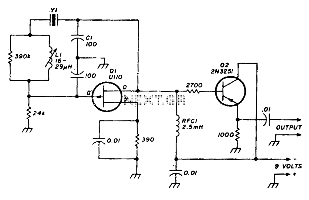
2. Direct Analog Synthesizers
2.1 Direct Analog Synthesizers
Direct analog synthesizers generate output frequencies through a series of analog signal processing stages, including mixing, multiplication, and division of a stable reference signal. Unlike digital synthesizers, they avoid phase-locked loops (PLLs) and instead rely on purely analog techniques to achieve fast switching speeds and low phase noise.
Fundamental Operating Principle
The core mechanism involves arithmetic manipulation of a high-stability reference oscillator, typically a crystal or atomic clock. The output frequency fout is derived by combining multiple reference-derived signals via:
where N and M are integer scaling factors, fref is the reference frequency, and Δf represents an offset introduced by mixing. The absence of feedback loops allows near-instantaneous frequency switching, limited only by propagation delays in analog components.
Key Components and Signal Flow
A typical architecture consists of:
- Reference oscillators – Ultra-low phase noise sources (e.g., 10 MHz OCXO).
- Frequency multipliers – Non-linear devices (step-recovery diodes or varactor-based) generating harmonics.
- Mixers – Double-balanced multipliers producing sum/difference frequencies.
- Bandpass filters – Suppress unwanted mixing products and harmonics.
- Switches/multiplexers – Select signal paths for different output frequencies.
Phase Noise Considerations
Phase noise performance follows the power-law relationship:
where fm is the offset frequency from the carrier. Multiplier stages degrade phase noise by 20log10(N) dB, making low-noise references critical. Typical systems achieve <-110 dBc/Hz at 1 kHz offset for X-band outputs.
Historical and Modern Applications
Early radar and jamming systems (1960s-1980s) extensively used direct synthesis for agility. Contemporary applications include:
- Electronic warfare (ECM) systems requiring microsecond-scale frequency hops
- Metrology-grade signal generators (e.g., Keysight 8663A)
- Quantum computing control systems where digital PLLs introduce unacceptable latency
Limitations and Trade-offs
While offering superior switching speed (<1 μs) and spur performance, direct synthesizers suffer from:
- Complexity scaling with frequency range (requires more mixer/filter stages)
- Higher power consumption than fractional-N PLLs
- Discrete frequency steps determined by reference dividers
where LCM denotes the least common multiple of divider ratios. This constraint makes fine resolution below 1 Hz impractical without prohibitively large M values.
2.2 Indirect Phase-Locked Loop (PLL) Synthesizers
Operating Principle
An indirect PLL-based frequency synthesizer generates stable output frequencies by locking the phase of a voltage-controlled oscillator (VCO) to a reference signal. The core components include:
- A phase detector (PD) comparing the reference and feedback phases.
- A loop filter (LF) suppressing high-frequency noise.
- A VCO generating the output frequency.
- A frequency divider (÷N) in the feedback path enabling programmable frequency steps.
Mathematical Model
The PLL's linearized phase-domain model is derived from the phase detector's output voltage \( V_d(t) \), proportional to the phase difference \( \phi_e(t) = \phi_{ref}(t) - \phi_{fb}(t) \). The loop filter’s transfer function \( F(s) \) shapes the dynamics:
The VCO’s output phase \( \phi_{out}(s) \) relates to its control voltage \( V_c(s) \) by:
With feedback division by \( N \), the closed-loop transfer function becomes:
Loop Filter Design
A second-order passive RC filter is common for stability and noise rejection. Its transfer function is:
where \( \tau_1 = R_1 C \), \( \tau_2 = R_2 C \), and \( \tau_3 = R_2 C_2 \). The loop bandwidth \( \omega_n \) and damping factor \( \zeta \) are:
Phase Noise and Spurs
Phase noise arises from VCO jitter, reference oscillator instability, and divider noise. Leakage currents in the charge pump create reference spurs at offsets of \( f_{ref} \). Spurs are mitigated by:
- Optimizing loop bandwidth to balance reference noise and VCO noise suppression.
- Using fractional-N synthesis with dithering to reduce integer-boundary spurs.
Fractional-N Synthesis
To achieve finer frequency resolution without reducing \( f_{ref} \), fractional-N dividers modulate the division ratio dynamically. A delta-sigma modulator shapes quantization noise, pushing it to higher frequencies where the loop filter attenuates it. The effective division ratio becomes:
where \( k \) is the fractional accumulator value and \( m \) is the modulator’s bit depth.
Applications
PLL synthesizers are critical in:
- Wireless communications: Local oscillators in 5G and Wi-Fi transceivers.
- Radar systems: Fast-switching frequency-agile sources.
- Test equipment: Signal generators with sub-Hz resolution.
2.3 Direct Digital Synthesizers (DDS)
Direct Digital Synthesizers (DDS) generate highly stable, programmable frequency signals by leveraging digital signal processing techniques. Unlike analog synthesizers, DDS relies on phase accumulation and digital-to-analog conversion to produce precise waveforms with minimal phase noise and fast switching times.
Phase Accumulator and Frequency Tuning
The core of a DDS is the phase accumulator, a digital integrator that increments a phase value at each clock cycle. The output frequency is determined by the phase increment value Δθ and the system clock frequency fclk:
where N is the bit width of the phase accumulator. Higher N enables finer frequency resolution, often reaching sub-Hertz levels in modern implementations.
Waveform Generation via Lookup Tables
The phase accumulator output addresses a waveform lookup table (LUT), which stores discrete amplitude values of the desired waveform (e.g., sine, square, or triangle). The LUT output is then converted to an analog signal via a high-speed digital-to-analog converter (DAC).
For a sine wave, the LUT stores values computed as:
where M is the LUT address width and Amax is the full-scale DAC output. Quantization errors due to finite M introduce harmonic distortion, which can be mitigated using interpolation techniques.
Spurious Signals and Noise Considerations
DDS outputs contain spurious signals caused by phase truncation, amplitude quantization, and DAC nonlinearities. The worst-case spurious-free dynamic range (SFDR) is approximated by:
Phase dithering and noise shaping techniques improve SFDR by randomizing quantization errors.
Applications and Modern Implementations
DDS is widely used in:
- Communications: Agile local oscillators in software-defined radios.
- Radar: Linear frequency modulation (chirp) generation.
- Test equipment: Arbitrary waveform generators with nanosecond switching.
Modern DDS ICs integrate 32-bit phase accumulators, 14-bit DACs, and on-chip DSP, achieving fout up to 1 GHz with sub-millihertz resolution.
Hybrid Synthesizers
Hybrid synthesizers combine the strengths of direct analog synthesis (DAS) and indirect phase-locked loop (PLL) synthesis to achieve superior spectral purity, fast switching speeds, and fine frequency resolution. These systems typically integrate a high-frequency PLL with a low-frequency direct digital synthesizer (DDS) or fractional-N divider, leveraging the advantages of both architectures while mitigating their individual limitations.
Architecture and Operating Principles
The core of a hybrid synthesizer consists of:
- A PLL-based coarse-tuning stage for wide frequency coverage and low phase noise.
- A DDS fine-tuning stage for sub-Hertz resolution and rapid frequency hopping.
- A mixing or offset loop to suppress spurious signals from the DDS.
The output frequency fout is derived from the sum or difference of the PLL (fPLL) and DDS (fDDS) outputs:
Phase Noise Analysis
The composite phase noise Ltotal(f) of a hybrid synthesizer is dominated by the PLL at small offset frequencies and the DDS at larger offsets. For a system with a mixing stage, the total noise power spectral density is:
where LPLL(f) follows Leeson's model and LDDS(f) is shaped by the digital quantization noise.
Spurious Suppression Techniques
Key methods to mitigate DDS-originated spurs include:
- High-side mixing to place spurs outside the band of interest.
- Phase dithering to randomize quantization errors.
- Bandpass filtering with tunable YIG or varactor-tuned filters.
Practical Implementations
Modern hybrid synthesizers achieve performance benchmarks such as:
- Phase noise below -110 dBc/Hz at 1 kHz offset (10 GHz carrier).
- Switching speeds under 10 µs for 1 MHz frequency steps.
- Spurious levels suppressed to -80 dBc or better.
These systems are deployed in radar, satellite communications, and quantum computing applications where both spectral purity and agility are critical.
Case Study: Microwave Backhaul Synthesizer
A 28 GHz 5G backhaul transceiver might employ a hybrid architecture with:
- A 7 GHz PLL using a GaN VCO for low 1/f noise.
- A 1 GS/s DDS providing 0.1 Hz resolution.
- A quadrupler chain to reach the final frequency.
This design achieves <-100 dBc/Hz phase noise at 100 kHz offset while maintaining <5 µs switching times between channel allocations.
3. Basic PLL Architecture and Components
Basic PLL Architecture and Components
A phase-locked loop (PLL) is a feedback control system that synchronizes the phase and frequency of an output signal with a reference input signal. The core architecture consists of four primary components: a phase detector (PD), a loop filter (LF), a voltage-controlled oscillator (VCO), and a frequency divider (FD). Each component plays a critical role in ensuring stable frequency synthesis and phase alignment.
Phase Detector (PD)
The phase detector compares the phase difference between the reference signal θref and the feedback signal θfb, generating an error signal proportional to their phase difference. Common implementations include:
- Analog multipliers (Mixers): Produce an output proportional to the product of the input signals, resulting in a DC component that varies with phase difference.
- Digital XOR gates: Generate a pulse-width modulated signal whose duty cycle corresponds to the phase difference.
- Phase-frequency detectors (PFDs): Offer both phase and frequency discrimination, essential for fast acquisition and reduced lock time.
The error signal Ve from the PD is given by:
where Kpd is the phase detector gain in volts per radian.
Loop Filter (LF)
The loop filter shapes the error signal to stabilize the PLL and suppress high-frequency noise. Its transfer function F(s) determines the system's dynamic response. Common configurations include:
- Passive RC filters: First-order low-pass filters with transfer function F(s) = 1/(1 + sRC).
- Active filters: Incorporate op-amps for higher gain and flexibility, such as the proportional-integral (PI) topology.
where τ1 and τ2 are time constants governing the PLL's bandwidth and damping factor.
Voltage-Controlled Oscillator (VCO)
The VCO generates the output signal with a frequency fout proportional to the control voltage Vctrl. Its linearized model is:
where f0 is the free-running frequency and Kvco is the gain in Hz/V. In practice, VCOs exhibit nonlinearities and tuning range limitations, necessitating careful design.
Frequency Divider (FD)
The frequency divider scales the VCO output by a factor N to match the reference frequency, enabling programmable frequency synthesis. The divider ratio N can be fixed or dynamically adjusted (e.g., in fractional-N PLLs). The feedback signal frequency is:
Integer-N dividers use counters, while fractional-N implementations employ delta-sigma modulation to achieve fine frequency resolution.
Closed-Loop Dynamics
The PLL's closed-loop transfer function H(s) relates the output phase θout to the reference phase θref:
For a second-order PLL with a PI loop filter, this simplifies to:
where ωn is the natural frequency and ζ is the damping ratio. These parameters dictate the PLL's lock time, bandwidth, and stability.
3.2 Loop Filter Design and Stability Considerations
The loop filter in a phase-locked loop (PLL) frequency synthesizer critically determines stability, phase noise, and settling time. Its design involves trade-offs between bandwidth, phase margin, and spur suppression. A well-designed filter ensures the PLL remains stable while meeting transient and spectral purity requirements.
Transfer Function and Stability Criteria
The loop filter's transfer function, F(s), shapes the open-loop gain G(s) of the PLL:
where KVCO is the VCO gain (Hz/V), KPD is the phase detector gain (A/rad), and N is the feedback divider ratio. The system's stability is governed by the phase margin (PM), typically targeted at 45°–60° for robust performance. The phase margin is derived from the open-loop phase response at the crossover frequency ωc:
Passive vs. Active Loop Filters
Passive filters (e.g., lag-lead) are simple and noise-resistant but lack DC gain, limiting lock range. A second-order passive filter has the form:
where τ2 = R2C and τ1 = (R1 + R2)C. Active filters (e.g., integrator-based) provide high DC gain and better spur suppression but introduce op-amp noise. A third-order active filter adds a pole for improved reference spur attenuation:
Design Procedure for a Stable Loop
- Determine bandwidth (ωc): Typically 1/10th to 1/20th of the reference frequency to avoid excessive reference spurs.
- Select phase margin: 50° is a common starting point for balancing stability and settling time.
- Calculate time constants: For a second-order filter, τ2 = sec(PM) - tan(PM)/ωc.
- Simulate open-loop response: Verify PM and gain margin (GM > 10 dB) in SPICE or MATLAB.
Nonlinear Effects and Jitter
Component tolerances and VCO pulling can degrade stability. Monte Carlo analysis helps quantify sensitivity to resistor/capacitor variations. Jitter peaking near ωc must be minimized to prevent timing violations in clocked systems.
Practical Considerations
- Capacitor leakage: High-quality ceramics or film capacitors reduce drift in τ2.
- Op-amp slew rate: Must exceed dV/dt during frequency hops to avoid transient lock failures.
- Layout parasitics: Stray capacitance at the VCO control node can unintentionally increase filter order.
Fractional-N and Integer-N PLLs
Fundamental Operation of Integer-N PLLs
Integer-N phase-locked loops (PLLs) derive their output frequency by multiplying a reference frequency fref by an integer divider value N. The output frequency fout is given by:
This architecture imposes a fundamental trade-off: channel spacing is equal to fref, while loop bandwidth must remain below fref/10 to maintain stability. For applications requiring fine frequency resolution (e.g., wireless communications), this forces undesirably low loop bandwidth, increasing settling time and phase noise.
Fractional-N PLL Architecture
Fractional-N PLLs overcome this limitation by allowing the divider ratio to take fractional values. The effective division ratio becomes:
where N is the integer part, K is the fractional numerator (0 ≤ K < F), and F is the fractional modulus. This enables channel spacing smaller than fref while maintaining higher loop bandwidth.
Sigma-Delta Modulation in Fractional-N PLLs
The fractional divider is implemented using a sigma-delta modulator (ΣΔM) that dynamically switches between integer divider values N and N+1. The ΣΔM shapes the quantization noise, pushing it to higher frequencies where it can be filtered by the PLL's low-pass characteristic. A first-order ΣΔM generates divider values according to:
where ε[n] represents the accumulated fractional error. Higher-order ΣΔ modulators (e.g., MASH 1-1-1) further improve noise shaping by cascading multiple first-order stages.
Phase Error and Spur Mechanisms
Fractional-N PLLs introduce two critical non-idealities:
- Fractional spurs: Result from periodic patterns in the ΣΔM output, creating discrete tones at offsets of fref/F from the carrier.
- Quantization noise: The ΣΔM's inherent quantization appears as phase noise, particularly problematic in higher-order modulators where out-of-band noise increases.
Advanced techniques like phase interpolation and digital spur cancellation are employed to mitigate these effects. Modern implementations achieve spur levels below -80 dBc with proper calibration.
Performance Comparison
The table below contrasts key parameters between Integer-N and Fractional-N PLLs:
| Parameter | Integer-N | Fractional-N |
|---|---|---|
| Frequency Resolution | fref | fref/F |
| Loop Bandwidth | ≤ fref/10 | ≤ fref/2 |
| Phase Noise Floor | Lower | Higher (due to ΣΔM) |
| Spurious Content | Reference spurs only | Fractional spurs |
Practical Implementation Considerations
Modern fractional-N synthesizers integrate several key components:
- Digital calibration: Compensates for charge pump mismatches that would otherwise exacerbate fractional spurs.
- Adaptive bandwidth control: Dynamically adjusts loop bandwidth during frequency transitions to optimize settling time.
- Noise cancellation: Digital-to-time converters (DTCs) subtract predicted quantization noise from the phase detector output.
These techniques enable fractional-N PLLs to achieve sub-Hz frequency resolution with settling times under 10 μs, making them indispensable in 5G NR and millimeter-wave systems.
Advanced PLL Techniques (All-Digital PLLs, Subsampling PLLs)
All-Digital Phase-Locked Loops (ADPLLs)
Traditional PLLs rely on analog components such as voltage-controlled oscillators (VCOs) and charge pumps, which introduce noise and process variations. All-digital PLLs (ADPLLs) replace these analog blocks with digital equivalents, improving robustness in scaled CMOS technologies. The core components of an ADPLL include:
- Digitally Controlled Oscillator (DCO): Replaces the VCO, with frequency tuning achieved through switched capacitor banks or varactor arrays controlled by a digital word.
- Time-to-Digital Converter (TDC): Measures the phase difference between the reference clock and the DCO output with picosecond resolution.
- Digital Loop Filter (DLF): Implements the loop dynamics using digital signal processing, allowing flexible bandwidth adjustment.
The phase error ϕe in an ADPLL is quantized by the TDC and processed by the DLF to generate the DCO tuning word. The loop dynamics can be modeled in the z-domain as:
where KDCO is the DCO gain, KTDC is the TDC gain, and F(z) represents the DLF transfer function. ADPLLs excel in applications requiring fast locking and low jitter, such as wireless transceivers and microprocessors.
Subsampling PLLs (SSPLLs)
Subsampling PLLs reduce phase noise by sampling the VCO output at a rate much lower than its oscillation frequency, effectively bypassing the divider chain's noise contribution. The key principle involves:
- Subsampling Phase Detector (SSPD): Directly samples the VCO output using the reference clock, producing a voltage proportional to the phase error.
- Charge Pump-Free Operation: The SSPD output drives the loop filter directly, eliminating charge pump noise.
The phase detector gain KPD in an SSPLL is derived from the VCO amplitude AVCO and the sampling slope:
where ωVCO is the VCO frequency and θslope is the sampling instant phase. SSPLLs achieve superior phase noise performance, making them ideal for millimeter-wave communications and high-precision clock generation.
Comparative Analysis
The choice between ADPLLs and SSPLLs depends on application constraints:
| Parameter | ADPLL | SSPLL |
|---|---|---|
| Phase Noise | Moderate (TDC-limited) | Excellent (divider noise avoided) |
| Power Consumption | Low (digital dominance) | Higher (RF sampling) |
| Lock Time | Fast (DLF programmability) | Slower (analog settling) |
Recent hybrid architectures combine ADPLL programmability with subsampling noise reduction, pushing the boundaries of integrated frequency synthesis.
4. DDS Architecture and Working Principle
4.1 DDS Architecture and Working Principle
Direct Digital Synthesis (DDS) is a frequency synthesis technique that generates precise, programmable waveforms using digital signal processing. The core components of a DDS system include a phase accumulator, a lookup table (LUT), and a digital-to-analog converter (DAC), followed by an anti-aliasing filter.
Phase Accumulator
The phase accumulator is a critical component that determines the output frequency. It operates as a modulo-N counter, where N is the number of bits in the accumulator. The phase increment (Δθ) is added to the accumulator at each clock cycle, producing a linearly increasing phase value:
where M is the bit width of the accumulator. The output frequency fout is determined by:
Here, fclk is the reference clock frequency. The frequency resolution is given by:
Lookup Table (LUT) and Waveform Generation
The phase accumulator's output serves as an address for the lookup table, which stores precomputed samples of the desired waveform (e.g., sine, square, or triangle). The LUT outputs a digital amplitude value corresponding to the phase angle, which is then converted to an analog signal by the DAC.
Digital-to-Analog Conversion and Filtering
The DAC converts the discrete amplitude values into an analog signal, but this introduces quantization noise and harmonics. An anti-aliasing low-pass filter is used to smooth the output and remove high-frequency artifacts. The filter's cutoff frequency must be set below the Nyquist frequency (fclk/2) to prevent aliasing.
Spurious Performance and Phase Truncation
In practical implementations, phase truncation occurs when the phase accumulator's output is truncated before addressing the LUT. This introduces spurious signals, degrading spectral purity. The spurious-free dynamic range (SFDR) is a key metric for DDS performance and is influenced by the number of bits in the phase accumulator and LUT.
Applications and Advantages
DDS is widely used in communications, radar, and instrumentation due to its fast frequency switching, fine resolution, and phase-continuous tuning. Modern implementations integrate DDS cores into field-programmable gate arrays (FPGAs) or application-specific integrated circuits (ASICs), enabling compact and high-performance solutions.
4.2 Phase Accumulator and Look-Up Table (LUT) Design
Phase Accumulator: Core of Direct Digital Synthesis (DDS)
The phase accumulator is a critical component in Direct Digital Synthesis (DDS) systems, responsible for generating a linear phase ramp that determines the output frequency. It operates as an N-bit modulo-M counter, where M = 2N defines the resolution of the phase steps. The output frequency fout is given by:
where fclk is the clock frequency, ΔP is the phase increment (tuning word), and N is the bit width of the accumulator. A larger N improves frequency resolution but increases hardware complexity.
Phase-to-Amplitude Conversion via LUT
The phase accumulator’s output is a digital phase value, which must be converted into an analog waveform. This is achieved using a Look-Up Table (LUT) that maps phase values to corresponding amplitude samples of the desired waveform (e.g., sine, triangle, or square). The LUT’s size and precision directly impact spurious performance and harmonic distortion.
For a sine wave, the LUT stores quantized samples of:
where K ≤ N is the number of address bits used to index the LUT. Truncating phase bits (N-K) introduces phase truncation spurs, while amplitude quantization adds noise.
Optimizing LUT Design
To minimize errors, several techniques are employed:
- Phase Dithering: Adds pseudo-random noise to reduce spurious tones caused by phase truncation.
- Amplitude Compression: Stores only a quarter-wave or half-wave sine sample, exploiting symmetry to reduce memory usage.
- Interpolation: Uses linear or polynomial interpolation between LUT entries to improve amplitude resolution without increasing table size.
Practical Implementation Trade-offs
In FPGA or ASIC implementations, the LUT is often implemented using block RAM (BRAM) or distributed memory. Key design considerations include:
- Memory Depth vs. Performance: A 12-bit LUT offers ~74 dBc SFDR (Spurious-Free Dynamic Range), while 16 bits exceed 100 dBc but require 4× more memory.
- Pipeline Latency: Adding pipeline stages improves clock speed but increases output latency.
- Nonlinear Correction: Predistortion can compensate for DAC nonlinearities in the analog output stage.
Case Study: High-Speed DDS with 32-Bit Phase Accumulator
A 32-bit accumulator (N=32) with a 1 GHz clock achieves a frequency resolution of:
Coupled with a 14-bit LUT and 16-bit DAC, this system achieves >80 dBc SFDR, suitable for communications and radar applications. Phase dithering reduces spurs by 10–15 dB at the cost of a slight noise floor increase.
4.3 Spurious Signals and Mitigation Techniques
Spurious signals, or spurs, are undesired frequency components that appear in the output spectrum of a frequency synthesizer. These artifacts degrade spectral purity and can interfere with adjacent channels, compromising system performance in communication and radar applications. Spurs arise from nonlinearities, phase noise, and intermodulation effects within the synthesizer architecture.
Sources of Spurious Signals
Spurs originate from several mechanisms:
- Reference Feedthrough: Leakage of the reference frequency (fref) into the output due to imperfect isolation in the phase-locked loop (PLL).
- Fractional-N Divider Artifacts: Quantization noise and periodic modulation in fractional-N synthesizers generate spurs at offset frequencies.
- Power Supply Coupling: Switching noise from regulators or digital circuits modulates the voltage-controlled oscillator (VCO).
- Nonlinear Mixing: Intermodulation between harmonics of the reference, divider, or VCO signals creates sum/difference spurs.
Mathematical Modeling of Spurs
The power level of a spur at an offset frequency Δf can be modeled as:
where K is a synthesizer-dependent constant, φn is the phase noise contribution, fref is the reference frequency, and C accounts for circuit-specific nonlinearities.
Mitigation Techniques
1. Loop Filter Optimization
A higher-order passive or active loop filter attenuates reference feedthrough and high-frequency noise. The transfer function of a 3rd-order filter is:
where τ1...4 are time constants set by resistor/capacitor values. Proper pole-zero placement reduces spurs by 20–40 dB.
2. Delta-Sigma Modulation in Fractional-N Synthesizers
High-order delta-sigma modulators (e.g., MASH-111) randomize divider modulus switching, converting spurs into shaped noise that is filtered by the PLL:
where N is the modulator order and E(z) is quantization noise.
3. Layout and Shielding
- Guard rings and separate ground planes for analog/digital sections reduce coupling.
- Low-noise LDO regulators suppress power supply-induced spurs.
- Symmetrical routing minimizes differential-mode interference.
4. Spur Cancellation Techniques
Adaptive algorithms inject anti-phase signals to cancel specific spurs. For a spur at fspur, the cancellation signal is:
This requires real-time detection via an auxiliary phase detector or spectrum analyzer.
Case Study: Cellular Base Station Synthesizer
In a 5G mmWave synthesizer (28 GHz), spurs at ±100 kHz offsets were reduced from -45 dBc to -72 dBc by:
- Implementing a 4th-order loop filter with fc = 50 kHz
- Using a 3rd-order delta-sigma modulator for fractional division
- Shielding the VCO with a Faraday cage
4.4 Advantages and Limitations of DDS
Advantages of Direct Digital Synthesis
Direct Digital Synthesis (DDS) offers several key advantages over traditional analog frequency synthesis techniques, making it a preferred choice in many high-performance applications.
- Exceptional Frequency Resolution: DDS systems achieve sub-Hertz frequency resolution, often limited only by the bit-width of the frequency tuning word (FTW). The step size Δf is given by:
$$ \Delta f = \frac{f_{clk}}{2^N} $$where fclk is the reference clock frequency and N is the phase accumulator bit width. For a 48-bit accumulator with a 1 GHz clock, this yields a theoretical resolution of ~3.55 μHz.
- Rapid Frequency Switching: Phase-continuous frequency transitions occur in a single clock cycle, typically in nanoseconds for modern DDS ICs. This makes DDS ideal for frequency-hopping spread spectrum systems and agile radar applications.
- Phase-Coherent Operation: The deterministic nature of digital phase accumulation ensures precise phase relationships between multiple DDS channels, critical for phased array systems and quadrature modulation.
- Digital Modulation Capabilities: DDS enables direct integration of complex modulation schemes (FSK, PSK, QAM) through real-time updates of the FTW, phase offset word, or amplitude scaling.
Inherent Limitations and Trade-offs
Despite its advantages, DDS technology faces several fundamental limitations that engineers must account for in system design:
- Spurious Frequency Generation: Phase truncation errors and amplitude quantization in the lookup table introduce spurious signals. The worst-case spur level relative to the carrier can be approximated by:
$$ P_{spur} \approx 6.02M + 1.76 \text{ dBc} $$where M is the number of phase bits truncated. A typical 14-bit DDS with 10 truncated bits yields spurs at -61.96 dBc.
- Nyquist Constraint: The maximum output frequency is theoretically limited to fclk/2, but practical implementations rarely exceed 40% of fclk due to reconstruction filter requirements. Higher frequencies introduce aliasing artifacts that degrade spectral purity.
- Power Consumption: High-speed DDS cores with large accumulators (>32 bits) and high-resolution DACs (>14 bits) can consume significant power, often exceeding 1W at multi-GHz clock rates.
- Phase Noise Limitations: While DDS eliminates analog PLL phase noise, the system inherits the reference clock's phase noise profile plus additional quantization noise:
$$ \mathcal{L}(f) = \mathcal{L}_{clk}(f) + 10\log\left(\frac{f_{clk}}{2f^2}\right) $$
Practical Mitigation Techniques
Advanced DDS implementations employ several techniques to overcome these limitations:
- Dithering: Adding controlled noise to the phase accumulator reduces spurious tones by randomizing quantization errors, at the cost of slightly increased noise floor.
- Interpolation: Digital upsampling combined with high-order FIR filters pushes aliased components further from the desired signal, relaxing analog filter requirements.
- Hybrid Architectures: Combining DDS with analog PLLs (as in the Digiphase technique) extends frequency range while maintaining fine resolution.
Application-Specific Considerations
In radar systems, DDS enables precise chirp generation with linearity better than 0.01% over wide bandwidths. For quantum computing applications, the phase coherence between multiple DDS channels (< 0.01° RMS) is critical for qubit control. Wireless test equipment leverages DDS for generating complex modulated signals with EVM better than -50 dB.
5. Component Selection (VCOs, Dividers, Mixers)
5.1 Component Selection (VCOs, Dividers, Mixers)
Voltage-Controlled Oscillators (VCOs)
The VCO is the core of a frequency synthesizer, generating an output signal whose frequency is controlled by an input voltage. The phase noise performance and tuning range are critical parameters. The phase noise of a VCO is modeled by Leeson's equation:
where F is the noise factor, k is Boltzmann's constant, T is temperature, Psig is the signal power, f0 is the center frequency, QL is the loaded quality factor, and fc is the flicker noise corner frequency. Higher QL reduces phase noise but narrows the tuning range.
Modern VCOs employ LC-tank or ring oscillator topologies. LC-tank VCOs offer superior phase noise but limited tuning range, while ring oscillators provide wide tuning at the cost of higher phase noise. For microwave applications, YIG-tuned or dielectric resonator oscillators (DROs) are preferred.
Frequency Dividers
Dividers reduce the VCO frequency to a lower value for phase comparison. The choice between integer and fractional-N dividers depends on the required frequency resolution and spurious performance.
Integer dividers use cascaded flip-flops in a synchronous or asynchronous configuration. The minimum achievable division ratio N is given by:
where n is the number of flip-flop stages. For fractional-N synthesis, delta-sigma modulators shape quantization noise away from the carrier frequency.
High-speed dividers (>10 GHz) often employ injection-locked or regenerative architectures. Silicon-germanium (SiGe) and gallium-arsenide (GaAs) technologies enable divider operation at mmWave frequencies.
Mixers for Frequency Translation
Mixers perform frequency translation by multiplying two input signals. The ideal mixer output contains sum and difference frequencies:
Key mixer specifications include conversion loss (or gain), isolation between ports, and third-order intercept point (IP3). Double-balanced mixers using Schottky diodes or Gilbert cell topologies provide excellent LO-RF isolation (>30 dB) and suppression of even-order harmonics.
For millimeter-wave applications, subharmonic mixers reduce LO frequency requirements by exploiting nonlinearities at harmonic frequencies. Monolithic microwave integrated circuits (MMICs) integrate mixers with VCOs and dividers for compact synthesizer solutions.
Component Selection Trade-offs
Selecting components involves balancing conflicting requirements:
- Phase noise vs. tuning range: High-Q resonators improve phase noise but limit tuning. Varactor diodes with high Cmax/Cmin ratios extend tuning range.
- Power consumption vs. speed: Bipolar dividers operate faster than CMOS but consume more power. Current-mode logic (CML) provides a compromise.
- Integration level vs. performance: Discrete components often outperform integrated solutions but increase board area and cost.
Advanced synthesizer designs employ co-simulation of electromagnetic (EM) models for passive components with transistor-level circuits to predict system-level performance before fabrication.
5.2 PCB Layout and Noise Reduction Strategies
Ground Plane Design
A solid ground plane is critical for minimizing noise in frequency synthesizers. The return current paths for high-frequency signals must be as short as possible to reduce parasitic inductance. A multi-layer PCB with dedicated ground layers is ideal, as it provides low-impedance return paths. Avoid splitting the ground plane beneath sensitive analog components, as this can create ground loops and introduce noise coupling. For mixed-signal designs, a single contiguous ground plane is often superior to partitioned analog and digital grounds, provided proper component placement and routing are followed.
Power Supply Decoupling
High-frequency synthesizers demand careful power supply decoupling to suppress switching noise. Place low-inductance ceramic capacitors (e.g., 100 nF X7R) as close as possible to the power pins of each active component. Bulk capacitance (10–100 µF) should be distributed across the board to handle lower-frequency ripple. The effectiveness of decoupling can be quantified by the impedance of the power distribution network (PDN):
where R, L, and C represent the parasitic resistance, inductance, and capacitance of the PDN. Minimizing ZPDN across the synthesizer's operating bandwidth ensures stable voltage delivery.
Signal Routing and Crosstalk Mitigation
Differential pairs should be used for high-frequency signals (e.g., LO outputs, reference clocks) to reject common-mode noise. Maintain consistent trace widths and spacing to preserve impedance matching. For microstrip lines, the characteristic impedance Z0 is given by:
where ϵr is the substrate dielectric constant, h is the height above the ground plane, w is the trace width, and t is the trace thickness. Isolate sensitive traces (e.g., VCO control lines) from noisy digital signals using guard traces or ground shielding.
Thermal Management
Phase-locked loops (PLLs) and voltage-controlled oscillators (VCOs) are sensitive to temperature fluctuations. Use thermal vias beneath high-power components (e.g., charge pumps) to dissipate heat to the ground plane or a dedicated thermal layer. The thermal resistance θJA can be approximated for a via array as:
where n is the number of vias, tsub is the substrate thickness, kCu is the thermal conductivity of copper, and Avia is the cross-sectional area of a single via.
Shielding and Filtering
For synthesizers operating in noisy environments, consider localized shielding cans over critical RF sections. Ferrite beads or π-filters can suppress conducted noise on power lines. The insertion loss of a filter is frequency-dependent and can be modeled as:
Measurements with a vector network analyzer (VNA) should validate filter performance across the synthesizer's tuning range.
Component Placement Strategies
Group functional blocks (e.g., PLL, VCO, dividers) to minimize interconnect lengths. Place the VCO away from digital sections and power regulators to reduce frequency pulling. Orient crystals and resonators perpendicular to high-current traces to mitigate microphonic effects. Use symmetric layouts for balanced circuits (e.g., differential amplifiers) to prevent phase imbalances.
5.3 Calibration and Tuning Techniques
Frequency synthesizers require precise calibration and tuning to maintain stability, minimize phase noise, and ensure accurate frequency generation. Advanced techniques leverage feedback loops, digital compensation, and adaptive algorithms to correct for component variations, temperature drift, and aging effects.
Phase-Locked Loop (PLL) Calibration
PLL-based synthesizers rely on calibration to optimize loop dynamics. The loop bandwidth ωn and damping factor ζ must be tuned to balance settling time and phase noise. For a second-order PLL with a charge pump, the loop filter components are derived from:
where KVCO is the VCO gain, ICP is the charge pump current, N is the division ratio, and R, C are the loop filter components. Automated calibration routines adjust ICP and R dynamically to maintain optimal performance.
Digital Predistortion for VCO Nonlinearity
Voltage-controlled oscillators exhibit nonlinear tuning characteristics, leading to frequency errors. Digital predistortion linearizes the KVCO curve by applying a polynomial correction:
where coefficients ak are determined during factory calibration using least-squares fitting. Real-time temperature compensation updates these coefficients via lookup tables.
Fractional-N Spurs Cancellation
Fractional-N synthesizers suffer from fractional spurs due to phase truncation. High-resolution sigma-delta modulators reduce quantization noise, while adaptive cancellation techniques inject anti-phase signals:
where weights wk are adapted using LMS algorithms. This reduces spurs by 20-40 dB in modern implementations.
Automatic Frequency Control (AFC)
AFC systems compensate for crystal oscillator drift by measuring the error between a reference (e.g., GPS) and the local oscillator. The correction voltage is computed as:
where Δf is the frequency error, and Kp, Ki are PID coefficients. Typical implementations achieve <1 ppb accuracy.
Temperature Compensation Techniques
OCXOs and MEMS oscillators use multi-point calibration across temperature ranges. The frequency deviation Δf(T) is modeled as:
where coefficients a, b, c are stored in non-volatile memory. Real-time sensors trigger polynomial evaluation, with residual errors <0.1 ppm.
Case Study: Cellular Base Station Synthesizer
LTE-A systems employ hybrid calibration with:
- Initial factory calibration: 32-point temperature sweep with vector network analyzer
- Online calibration: Pilot tone analysis with FFT-based spur detection
- Adaptive tuning: Reinforcement learning for VCO bank selection
This achieves <100 fs RMS jitter at 3.6 GHz with 50 μs settling time.
6. Key Research Papers and Books
6.1 Key Research Papers and Books
- PDF 6 Models and Analysis Techniques for Systematic Design And — This chapter describes both the necessary models and the simulation algorithm for the design and verification of frequency synthesizers used for telecommunication ap-plications. The chapter is organized as follows. Section 6.1 introduces the different as-pects that have to be taken into account when developing a model library. Section 6.2 concentrates on the application domain of frequency ...
- James A. Crawford - Frequency Synthesizer Design Handbook (1994 ... — For a complete listing of the Artech House Microwave Library, turn to the back of this book ffJames A. Crawford ffffTo Linda, Brian, James, Daniel, and Kristen To God be all the glory Hebrews 2:1-3 ffPreface xiii Chapter 1 Introduction to Computer-Aided Frequency Synthesizer Design 1 References 2 Chapter 2 Building Blocks for Frequency Synthesis Using Phase-Locked Loops 3 2.1 The Design ...
- CMOS PLL Synthesizers: Analysis and Design | SpringerLink — It works as a local oscillator for frequency translation and channel selection in wireless transceivers and broadband cable tuners. It also plays an important role as the clock synthesizer for data converters in the analog-and-digital signal interface. This book covers the design and analysis of PLL synthesizers.
- PDF Integrated Radio Frequency Synthesizers for Wireless Applications — Abstract This thesis consists of six publications and an overview of the research topic, which is also a summary of the work. The research described in this thesis concentrates on the design of phase-locked loop radio frequency synthesizers for wireless applications. In particular, the focus is on the implementation of the prescaler, the phase detector, and the chargepump.
- Integrated frequency synthesizers for wireless systems - Academia.edu — The increasingly demanding performance requirements of communications systems, as well as problems posed by the continued scaling of silicon technology, present numerous challenges for the design of frequency synthesizers in modern transceivers. This book contains everything you need to know for the efficient design of frequency synthesizers for today's communications applications. If you need ...
- PDF Integrated Frequency Synthesizers for Wireless Systems — Integrated Frequency Synthesizers for Wireless Systems The increasingly demanding performance requirements of communications systems, as well as prob-lems posed by the continued scaling of silicon technology, present numerous challenges for the design of frequency synthesizers in modern transceivers.
- A Frequency Synthesizer With Frequency — 4At frequency offsets that are multiple of the frequency of the periodic sawtooth signal. 5Based on the number of research works prevalent in the literature. Table 2.3: Examples of EA fractional frequency synthesizers.
- PDF Cmos Single Chip Fast Frequency Hopping Synthesizers for Wireless Multi ... — In this book, the authors outline detailed design methodology for fast frequency hopping synthesizers for radio frequency (RF) and wireless communications applications.
- PDF Phase Lock Loops and Frequency Synthesis — Special care is given to the problem of the phase-locked loop frequency synthesizers in the high-megahertz and low-gigahertz ranges where modern mobile communica-tions are placed.
- PDF Design of a sub-Hz Resolution Fully Digital RF Frequency Synthesizer — The Flying Adder Frequency Synthesizer prin-ciple of operation of the synthesizer are initially presented. This mathematical analysis shows the advantages (large tuning range and fine frequency resolution) that make this architecture suitable for our application, but also brings forth the main drawback of this ar
6.2 Online Resources and Datasheets
- FS2 Frequency Synthesizers | Keysight — Compact frequency synthesizers FS2 frequency synthesizers offer fast switching speed, low phase noise, and high output power in a variety of compact modules optimized for system integration. With models covering frequencies from 8 kHz to 40 GHz, FS2 frequency synthesizers can be used for a variety of applications, from general-purpose signal sources to radar, electronic warfare, and quantum ...
- ADF4156 Datasheet and Product Info | Analog Devices — The ADF4156 is a 6.2 GHz fractional-N frequency synthesizer that implements local oscillators in the up-conversion and down-conversion sections of wireless receivers and transmitters. It consists of a low noise digital phase frequency detector (PFD), a precision charge pump, and a programmable reference divider.
- A novel 0.72-6.2GHz continuously-tunable ΔΣ fractional-N frequency ... — This paper presents a wideband ΔΣ-based fractional-N synthesizer with three integrated quadrature VCOs for multiple-input multiple-output (MIMO) wireless communication applications. It continuously covers a wide range frequency from 0.72 GHz to 6.2 GHz that is suitable for multiple communication standards. The synthesizer is designed in 0.13-μm RF CMOS process. The dual clock full ...
- PDF ADF4156 (Rev. B) - Analog — The ADF4156 is a 6.2 GHz fractional-N frequency synthesizer that implements local oscillators in the upconversion and downconversion sections of wireless receivers and transmitters. It consists of a low noise digital phase frequency detector (PFD), a precision charge pump, and a programmable reference divider.
- PDF 6.2 GHz Fractional -N Frequency Synthesizer Data Sheet ADF4156 — For example, in a GSM 1800 system, 1.8 GHz RF frequency output (RFOUT) is required, 13 MHz reference frequency input (REFIN) is available, and 200 kHz channel resolution (fRES) is required on the RF output.
- Find Datasheets, Electronic Parts, Components - Datasheets.com — Datasheets.com is the easiest search engine to find datasheets of electronic parts. Search millions of components across thousands of manufacturers.
- Frequency Synthesizers Specifications - GlobalSpec — Find Frequency Synthesizers on GlobalSpec by specifications. Frequency synthesizers are electronic devices that generate frequencies by using a combination of other frequencies.
- PDF Programmable Frequency Scan Waveform Generator — The frequency profile is defined by the start frequency (FSTART), the frequency increment (Δf) and the number of increments per scan (NINCR). The increment interval between frequency increments, tINT, is either user-programmable with the interval automatically determined by the device (auto-increment mode), or externally controlled via a ...
- PDF LMK61E2 Ultra-Low Jitter Programmable Oscillator With Internal EEPROM — The LMK61E2 device is an ultra-low jitter PLLatinumTM programmable oscillator with a fractional-N frequency synthesizer with integrated VCO that generates commonly used reference clocks.
- PDF LMX8410L High-Performance Mixer With Integrated Synthesizer — The LMX8410L has a high level of integration providing high performance while saving board space and complexity. It integrates a wideband RF input balun, eliminating the need for external baluns. It integrates a high-performance PLL and VCO, eliminating the need for external LO and LO driver. The device also integrates an IF amplifier and several low noise LDOs, further simplifying the board.
6.3 Simulation Tools and Design Software
- PDF 6 Models and Analysis Techniques for Systematic Design And — This chapter describes both the necessary models and the simulation algorithm for the design and verification of frequency synthesizers used for telecommunication ap-plications. The chapter is organized as follows. Section 6.1 introduces the different as-pects that have to be taken into account when developing a model library. Section 6.2 concentrates on the application domain of frequency ...
- James A. Crawford - Frequency Synthesizer Design Handbook (1994 ... — For a complete listing of the Artech House Microwave Library, turn to the back of this book ffJames A. Crawford ffffTo Linda, Brian, James, Daniel, and Kristen To God be all the glory Hebrews 2:1-3 ffPreface xiii Chapter 1 Introduction to Computer-Aided Frequency Synthesizer Design 1 References 2 Chapter 2 Building Blocks for Frequency Synthesis Using Phase-Locked Loops 3 2.1 The Design ...
- EMX Designer - Cadence Design Systems — Overview Rapid, Versatile Passive Component Synthesis and Optimization Cadence EMX Designer provides faster and more flexible passive component synthesis and optimization than traditional software tools. Leveraging the proven accuracy of EMX 3D Planar Solver's electromagnetic (EM) modeling engine, EMX Designer takes split seconds to produce accurate, DRC-clean parametric cells (PCells) of ...
- A fractional-N frequency synthesizer with phase synchronization and ... — Section 5 reveals the implementation principle and circuit design of the programmable phase control. Section 6 shows the layout of the frequency synthesizer, as well as simulation results and analysis. Finally, the conclusion of this work is summarized in Section 7.
- COMSOL Multiphysics® Software - Understand, Predict, and Optimize — To help keep models and applications organized, the COMSOL Multiphysics ® platform also includes the Model Manager, which is a tool for modeling and simulation management that provides version control and efficient storage. Any combination of add-on products from the COMSOL product suite can be added to the COMSOL Multiphysics ® software ...
- PDF Predicting the Phase Noise and Jitter of PLL-Based Frequency Synthesizers — This is par-ticularly true with frequency synthesizers, especially those with large multiplication fac-tors. The problem is that a circuit simulator must use at least 10-20 time points for every period of the VCO for accurate rendering, and the lock process often involves hundreds or thousands of cycles at the input to the phase detector.
- PDF CST Studio Suite - Massachusetts Institute of Technology — CST Studio Suite for High Frequency Simulation is a fully featured software package for electromagnetic analysis and design in the high frequency range. It simplifies the process of creating the structure by providing a powerful graphical solid modeling front end which is based on the ACIS modeling kernel.
- PDF RF System DesignGuide - Keysight — The DesignGuide provides a complete tool kit to interactively explore Transmitter/Receiver systems at the top level as part of an integrated design process. In addition to the requirements of the Agilent EEsof ADS software, the RF System DesignGuide requires approximately 60 MBytes of additional storage space.
- PDF Design of a sub-Hz Resolution Fully Digital RF Frequency Synthesizer — The FA synthesizer using a first order EFM modulator has been theoretically analyzed in 3.2, 3.3, where simulation results have also been provided, motivating the investigation of higher order MASH modulators.
- PDF A Guide to Phase Noise Analysis of Single and Multi-PLL Frequency ... — 4 Phase 5 Phase 6 Spice Noise Simulation Representation 6.1 Example: Modeling a low-noise VCO