Hall Effect Sensors
1. The Hall Effect: Basic Theory and Discovery
The Hall Effect: Basic Theory and Discovery
In 1879, Edwin Hall discovered that when a current-carrying conductor is placed in a perpendicular magnetic field, a voltage develops across the conductor transverse to both the current and the field. This phenomenon, now known as the Hall effect, arises due to the Lorentz force acting on charge carriers in the material.
Physical Mechanism
Consider a thin conductive plate with current I flowing along the x-axis and a magnetic field B applied along the z-axis. The Lorentz force FL deflects charge carriers (electrons or holes) perpendicular to both current and field:
where q is the charge, v is the drift velocity, and E is the electric field. The transverse deflection creates charge accumulation on opposite edges, establishing an electric field EH that balances the Lorentz force at equilibrium:
Hall Voltage Derivation
The Hall voltage VH appears across the width w of the conductor. Relating drift velocity to current density J = nqvd, where n is charge carrier density, gives:
For a conductor of thickness t, current density J = I/(w × t). Substituting yields the fundamental Hall voltage equation:
where RH = 1/(nq) is the Hall coefficient, whose sign indicates the carrier type (negative for electrons, positive for holes).
Material Considerations
The Hall effect's magnitude depends critically on material properties:
- Semiconductors (Si, GaAs, InSb) exhibit larger effects than metals due to lower n
- Mobility (μ = vd/E) determines sensitivity - high mobility materials like graphene show exceptional response
- Temperature effects must be compensated in precision applications due to n and μ variations
Historical Context and Modern Significance
Hall's original experiment used gold foil in a 1.8 T electromagnet, measuring microvolt-level signals. Today, the effect enables:
- Non-contact current sensing in power electronics
- Precision position and speed detection in automotive systems
- Magnetic field mapping in scientific instruments
- Material characterization (carrier type, density, mobility)
Modern Hall sensors leverage semiconductor technology to achieve sensitivities exceeding 100 mV/T with integrated signal conditioning circuits. The quantum Hall effect, discovered in 2D electron systems at low temperatures, now defines the ohm in metrology.
How Hall Effect Sensors Work
The operation of Hall effect sensors is rooted in the fundamental physics of charge carriers moving through a conductor or semiconductor under the influence of electric and magnetic fields. When a current-carrying conductor is placed in a magnetic field perpendicular to the current flow, charge carriers experience a Lorentz force, leading to a measurable voltage difference across the conductor—the Hall voltage.
Lorentz Force and Charge Carrier Deflection
The Lorentz force acting on a charge carrier with charge q moving with velocity v in a magnetic field B is given by:
This force causes electrons (or holes) to accumulate on one side of the conductor, creating an electric field E that opposes further charge buildup. At equilibrium, the electric force balances the magnetic force:
Derivation of Hall Voltage
The Hall voltage VH arises due to the transverse electric field. For a conductor of thickness d, the Hall voltage is:
Expressing drift velocity v in terms of current density J and charge carrier density n (J = nqv), we obtain:
where I is the applied current and t is the thickness of the conductor in the direction of the magnetic field.
Material Considerations
The sensitivity of a Hall effect sensor depends on the material's charge carrier mobility and density. Semiconductors like gallium arsenide (GaAs) or indium antimonide (InSb) are preferred over metals due to their higher electron mobility and lower carrier concentration, resulting in larger Hall voltages for the same magnetic field strength.
Practical Sensor Configurations
Modern Hall effect sensors integrate amplification and signal conditioning circuitry to produce a usable output. Key configurations include:
- Linear sensors: Provide an analog output voltage proportional to the magnetic field strength.
- Threshold sensors: Digital output that switches state when the magnetic field exceeds a predefined level.
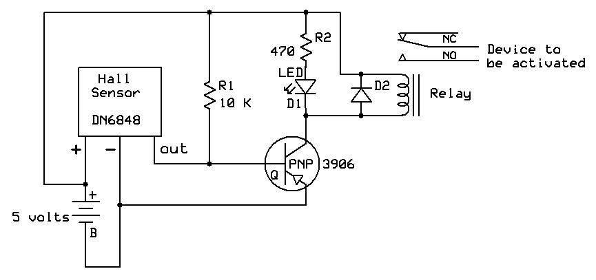
- Current sensors: Measure current by detecting the magnetic field around a conductor.
Temperature Compensation
Since semiconductor properties vary with temperature, high-precision Hall sensors incorporate temperature compensation circuits. This is typically achieved through:
- On-chip temperature sensors
- Feedback loops adjusting bias current
- Differential configurations canceling common-mode drift
Noise and Sensitivity Optimization
The signal-to-noise ratio in Hall sensors is maximized by:
where μ is carrier mobility, kB is Boltzmann's constant, T is temperature, and R is sensor resistance. Techniques like spinning current methods and chopper stabilization are employed to reduce 1/f noise.
Applications in Precision Measurement
High-end Hall sensors achieve resolutions below 50 μT, enabling applications in:
- Brushless motor commutation
- Precision current sensing in power electronics
- Contactless position detection in industrial automation
- Magnetic field mapping in scientific instruments
Types of Hall Effect Sensors: Analog vs. Digital
Hall effect sensors are broadly categorized into analog and digital types, each with distinct operational principles, output characteristics, and application domains. The choice between them depends on factors such as required resolution, noise immunity, and system interface compatibility.
Analog Hall Effect Sensors
Analog Hall sensors produce a continuous voltage output proportional to the magnetic flux density (B) perpendicular to the sensor surface. The output voltage (Vout) follows the linear relationship:
where SH is the sensitivity (typically in mV/mT) and Vq is the quiescent output voltage at zero magnetic field. The linearity of this response is governed by the material properties of the Hall element and the stability of the biasing current. High-performance analog sensors, such as the Allegro A1324, achieve sensitivities of 5 mV/mT with nonlinearity below 1%.
Key applications include:
- Precision current sensing in power electronics, where the sensor measures the field generated by a current-carrying conductor
- Position tracking in industrial automation, utilizing the linear displacement-to-field relationship
- Magnetometry for scientific instruments requiring analog field strength measurements
Digital Hall Effect Sensors
Digital Hall sensors incorporate internal thresholding circuitry to provide discrete output states, typically open-drain or push-pull logic levels. They employ Schmitt trigger architectures with hysteresis (BHYS) to prevent output oscillation near the switching point. The transfer function is characterized by:
where BOP is the operate point, BRP the release point, and BHYS = BOP - BRP. Modern digital Hall ICs like the Texas Instruments DRV5023 achieve sub-millitesla switching thresholds with 5 mT hysteresis.
Dominant use cases include:
- Revolution counting in automotive wheel speed sensors (ABS systems)
- End-position detection in brushless DC motor commutation
- Tamper-proofing in security systems via magnetic switch triggers
Comparative Analysis
The noise characteristics fundamentally differ between the two types. Analog sensors exhibit a signal-to-noise ratio (SNR) given by:
where Vn is the RMS noise voltage. Digital sensors, however, are immune to amplitude noise once the signal exceeds the hysteresis window, making them preferable in electrically noisy environments like automotive applications.
Power consumption represents another critical distinction. Analog sensors typically draw 5-10 mA continuous current for stable biasing, while digital variants with duty-cycled operation (e.g., Melexis MLX90392) can achieve average currents below 10 μA—a decisive advantage for battery-powered systems.
Recent advancements in CMOS-integrated Hall sensors blur this dichotomy, with devices like the AMS AS5600 combining 12-bit analog-to-digital conversion with programmable digital interfaces while maintaining 0.5° angular resolution for magnetic encoders.
2. Sensitivity and Output Voltage
Sensitivity and Output Voltage
The sensitivity of a Hall effect sensor is a critical parameter that quantifies its ability to convert a magnetic field into an electrical signal. It is defined as the ratio of the output voltage (VH) to the applied magnetic flux density (B), typically expressed in millivolts per tesla (mV/T). For high-precision applications, optimizing sensitivity is essential to ensure accurate detection of weak magnetic fields.
Mathematical Derivation of Hall Voltage
The Hall voltage (VH) arises due to the Lorentz force acting on charge carriers in a conductor or semiconductor subjected to a perpendicular magnetic field. Starting from the Lorentz force equation:
where q is the charge of the carrier, E is the electric field, v is the carrier drift velocity, and B is the magnetic flux density. At equilibrium, the transverse electric field balances the magnetic force, yielding:
Integrating the electric field across the width of the sensor (w) gives the Hall voltage:
Substituting the drift velocity vx = I/(nqA), where I is the bias current, n is the carrier concentration, and A = t · w is the cross-sectional area (t being the thickness), we arrive at the fundamental Hall voltage equation:
Sensitivity and Key Parameters
The sensitivity (S) is derived from the Hall voltage equation:
This reveals that sensitivity is directly proportional to the bias current I and inversely proportional to the carrier concentration n and sensor thickness t. Practical implications include:
- Material selection: Semiconductors (e.g., GaAs, InSb) offer higher sensitivity than metals due to lower carrier concentrations.
- Geometry optimization: Thin-film sensors maximize sensitivity by minimizing t.
- Bias current trade-offs: Increasing I improves sensitivity but raises power dissipation and self-heating effects.
Nonlinearity and Temperature Dependence
In real-world applications, sensitivity is not perfectly linear due to material inhomogeneities and parasitic effects. The output voltage may deviate as:
where S0 is the nominal sensitivity, α accounts for quadratic nonlinearity, and ε(T) represents temperature-dependent drift. Compensation techniques include:
- Differential sensor configurations to cancel even-order nonlinearities.
- Temperature-stabilized bias circuits using thermistors or proportional-to-absolute-temperature (PTAT) current sources.
Practical Measurement Considerations
For precision applications, the output voltage must be amplified and filtered. A typical signal chain includes:
- Low-noise amplifiers (LNA): To boost millivolt-level Hall voltages without introducing significant thermal noise.
- Bandpass filtering: To suppress 1/f noise and external interference.
- Offset nulling: Using spinning-current techniques to eliminate residual voltage due to fabrication asymmetries.
The figure illustrates a representative Hall voltage response curve, showing linear behavior at low fields and saturation effects at high flux densities.
2.2 Operating Voltage and Current Requirements
Supply Voltage Range
The operating voltage range of a Hall effect sensor is determined by its internal semiconductor structure and biasing requirements. Most integrated Hall sensors operate within 3.3V to 24V, with common industrial devices standardized at 5V or 12V. The minimum voltage Vmin must exceed the sum of the Hall element's intrinsic voltage drop and any required overhead for signal conditioning circuits:
where VHall is the Hall plate bias voltage (typically 1.2-2.5V), Vamp the amplifier headroom (0.5-1.5V), and Vreg any internal regulator dropout (0.3-1V). High-voltage variants (up to 60V) use on-chip voltage regulators or depletion-mode FETs.
Quiescent Current
The zero-field supply current IQ is dominated by the Hall plate bias current and amplifier consumption. For a typical bipolar Hall sensor:
Modern CMOS sensors achieve IQ below 5µA through switched biasing techniques, where the Hall plate is pulsed at 10-100kHz rather than continuously biased. This reduces power dissipation while maintaining bandwidth through sample-and-hold amplification.
Dynamic Current Requirements
Output stage current depends on the sensor type:
- Open-collector outputs sink current (e.g., 5-20mA) through an external pull-up resistor
- Push-pull CMOS outputs source/sink current limited by transistor sizing (typically 10-50mA)
- Analog output stages require 1-5mA for driving resistive/capacitive loads
For PWM-output sensors, the dynamic current Idyn includes switching losses:
Thermal Considerations
Junction temperature rise must be calculated for high-current applications. The power dissipation PD in a linear output sensor driving a load RL is:
Package thermal resistance (θJA) then determines the maximum permissible ambient temperature. For example, a SOT-23 package with θJA=206°C/W running at 150mW will experience a 31°C rise above ambient.
Voltage Transient Protection
Automotive and industrial sensors incorporate TVS diodes and RC filters to withstand ISO-7637-2 transients. The clamping voltage VCL must satisfy:
where VBR is the sensor's absolute maximum rating (typically 28-40V) and Vmargin a 10-20% safety buffer. Series resistors limit inrush current during load dump events (100V/100ms).
2.3 Temperature Dependence and Compensation
The performance of Hall effect sensors is significantly influenced by temperature variations, primarily due to the temperature-dependent properties of semiconductor materials. The key parameters affected include the Hall coefficient (RH), carrier mobility (μ), and intrinsic carrier concentration (ni). These dependencies introduce drift in the sensor's output voltage (VH), necessitating compensation techniques for stable operation.
Temperature Dependence of Hall Coefficient
The Hall coefficient (RH) exhibits a strong temperature dependence, governed by the relationship:
where n(T) is the temperature-dependent carrier concentration and q is the electron charge. In extrinsic semiconductors, n(T) follows an exponential trend:
where Eg is the bandgap energy and k is Boltzmann's constant. This results in a nonlinear decrease in RH with increasing temperature.
Mobility and Resistivity Effects
Carrier mobility (μ) decreases with temperature due to increased phonon scattering, following a power law:
This reduction in mobility directly impacts the sensor's sensitivity, as the Hall voltage is proportional to μ:
Simultaneously, the material resistivity (ρ) increases with temperature, affecting the input current and power dissipation.
Compensation Techniques
Modern Hall sensors employ several compensation strategies to mitigate temperature effects:
- Current Source Compensation: Using a temperature-dependent current source that varies inversely with mobility to maintain constant sensitivity.
- Differential Sensor Configuration: Pairing two Hall elements with opposite temperature coefficients to cancel out drift.
- On-Chip Temperature Sensors: Digital compensation using polynomial correction algorithms based on real-time temperature measurements.
- Material Engineering: Using compound semiconductors (e.g., InSb, GaAs) with flatter temperature characteristics than silicon.
Mathematical Compensation Example
A common digital compensation approach uses a second-order polynomial:
where α and β are calibration coefficients determined during sensor characterization. Advanced implementations may use piecewise linear approximation or neural networks for higher accuracy.
Practical Implementation Considerations
In integrated Hall sensors, compensation circuits typically occupy 30-50% of the die area. The effectiveness of compensation is limited by:
- Non-uniform temperature distribution across the chip
- Hysteresis effects in magnetic materials
- Nonlinearities in the temperature characteristics
State-of-the-art automotive-grade sensors achieve temperature stability of ±0.5% over -40°C to 150°C through a combination of analog and digital compensation techniques.
3. Position and Proximity Sensing
Position and Proximity Sensing
Fundamental Principles
Hall Effect sensors exploit the Lorentz force acting on charge carriers in a semiconductor under an applied magnetic field. When a current I flows through the sensor and a perpendicular magnetic field B is present, the resulting Hall voltage VH is given by:
where n is charge carrier density, e is electron charge, t is sensor thickness, and RH is the Hall coefficient. For position sensing, the magnetic field gradient dB/dx becomes the critical parameter, as VH varies linearly with displacement when operating within the sensor's linear range.
Linear Position Sensing
In linear displacement measurement, a moving magnet creates a spatially varying field. The Hall sensor's output voltage maps directly to position when:
- The magnet's pole orientation is parallel to the sensor plane
- The travel range is within ±50% of the magnet's pole pitch
- Temperature compensation is applied (via integrated circuits in modern sensors)
High-resolution applications (e.g., CNC machines) often use differential Hall sensor arrays with sub-micron resolution by interpolating between multiple sensor outputs.
Rotary Position Encoding
For angular measurement, two primary configurations exist:
- Axial magnetization: The magnet rotates parallel to the sensor plane, producing a sinusoidal VH variation. Resolution is enhanced by using arctangent calculation on quadrature outputs from orthogonal sensors.
- Radial magnetization: A multipole ring magnet passes over the sensor, generating discrete pulses for incremental encoding. The angular resolution Δθ is given by:
where N is magnet pole pairs and n is interpolation factor.
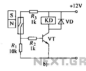
Proximity Detection
Binary proximity switches leverage the Hall Effect's threshold behavior. When B exceeds a critical value BOP, the output transistor switches states. Key design parameters include:
| Parameter | Typical Range | Effect on Performance |
|---|---|---|
| Operate Point (BOP) | 3-100 mT | Determines activation distance |
| Hysteresis (BHYST) | 1-20 mT | Prevents chatter in noisy environments |
Latching variants use alternating magnetic polarities, maintaining state until field reversal occurs - ideal for gear tooth counting and revolution tracking.
Error Sources and Compensation
Nonlinearity in position sensing primarily arises from:
- Magnetic field inhomogeneity (≥1% error)
- Temperature drift of sensitivity (0.02-0.2%/°C)
- Mechanical misalignment (cosine error)
Modern IC-based sensors implement on-chip compensation through:
where α and β are temperature coefficients calibrated during fabrication. Orthogonal field rejection (≥20 dB) is achieved through differential sensing architectures.
3.2 Current Measurement Techniques
Open-Loop vs. Closed-Loop Configurations
Hall effect sensors measure current by detecting the magnetic field generated around a current-carrying conductor. Two primary configurations exist: open-loop and closed-loop. In open-loop systems, the Hall sensor is placed in a fixed air gap near the conductor, and the output voltage is directly proportional to the magnetic field. Closed-loop systems employ a feedback coil to nullify the magnetic field, improving linearity and temperature stability at the cost of increased complexity.
Here, VH is the Hall voltage, KH the sensitivity coefficient, I the current, and B the magnetic flux density. Open-loop systems suffer from nonlinearities due to core saturation and temperature drift, whereas closed-loop systems mitigate these via feedback:
Core Selection and Magnetic Circuit Design
The magnetic core material (e.g., ferrite, permalloy) significantly impacts sensor performance. Core permeability (μr) and saturation flux density (Bsat) dictate the measurable current range. A high-μr core concentrates flux, enhancing sensitivity but risking saturation at high currents. The core geometry (toroidal, E-core) must minimize air gaps to reduce flux leakage.
Error Sources and Compensation Techniques
Key error sources include:
- Temperature drift: Affects Hall coefficient (RH) and core permeability. Compensate using temperature-stable materials or active circuitry (e.g., PTAT current sources).
- Offset voltage: Caused by misalignment or mechanical stress. Nullified via spinning-current techniques or auto-zero amplifiers.
- External fields: Shield with high-μ materials or use differential sensor pairs.
High-Frequency and Pulsed Current Measurement
For AC or pulsed currents, core eddy currents and hysteresis introduce phase lag and distortion. Laminated cores or nanocrystalline materials reduce losses. The bandwidth (f3dB) is limited by:
where R is the feedback resistor and L the coil inductance. High-speed applications (e.g., power electronics) often use Rogowski coils or integrated Hall ICs with >100 kHz bandwidth.
Practical Applications
- Motor drives
- Energy metering: Open-loop sensors provide galvanic isolation in smart meters.
- Fault detection: Fast-response Hall sensors detect short-circuit currents in protection circuits.
3.3 Speed Detection in Rotational Systems
Hall effect sensors enable precise non-contact speed measurement in rotational systems by detecting the passage of magnetic poles or ferromagnetic targets. The underlying principle relies on the periodic voltage pulses generated as a rotating element, such as a gear or encoder wheel, modulates the magnetic field sensed by the Hall element. The frequency of these pulses is directly proportional to the rotational speed.
Fundamental Theory
For a rotating disk with N equidistant magnetic poles or teeth, the angular velocity ω (in radians per second) relates to the pulse frequency f as:
Linear speed v at radius r follows from v = ωr. The sensor's output signal transitions between high and low states each time a pole passes, creating a square wave whose period T yields f = 1/T.
Implementation Considerations
Magnetic Field Alignment: Optimal sensitivity requires the magnetic flux lines to be perpendicular to the Hall element. Radial magnetization patterns in multipole rings minimize alignment errors.
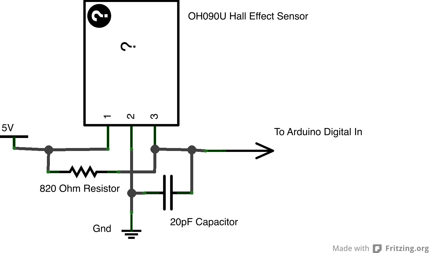
Signal Conditioning: Schmitt triggers or comparators convert the analog Hall voltage into digital pulses, while hysteresis suppresses noise. For high-resolution applications, interpolation techniques improve edge detection accuracy.
Error Sources and Compensation
- Eccentricity: Misalignment between the sensor and rotational axis introduces periodic errors. Dual-sensor configurations with quadrature output enable compensation.
- Temperature Drift: Hall coefficient and magnetic field strength vary with temperature. Integrated temperature sensors or differential measurements mitigate this effect.
- Jitter: Mechanical vibration or uneven pole spacing causes timing uncertainty. Digital filtering (e.g., moving average) improves stability.
Advanced Techniques
For ultra-high precision, time-stamping methods measure intervals between edges with resolution down to nanoseconds. Combining Hall sensors with optical encoders achieves hybrid systems with both high speed and absolute position tracking.
where fclock is the reference oscillator frequency. Real-time processing units (e.g., FPGA or dedicated timer peripherals) capture timestamps without software latency.
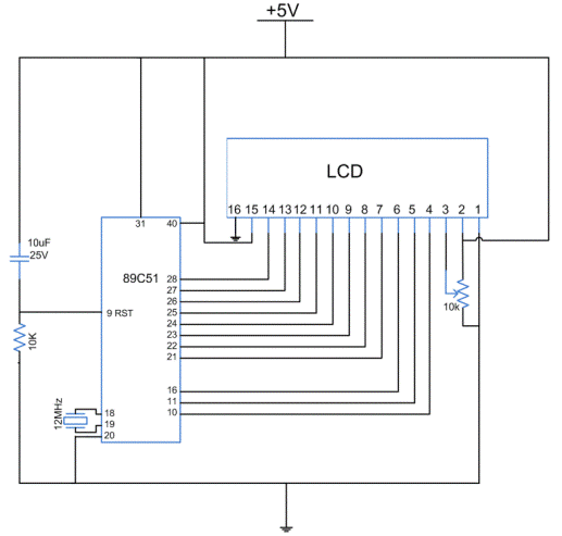
4. Interfacing Hall Effect Sensors with Microcontrollers
4.1 Interfacing Hall Effect Sensors with Microcontrollers
Hall effect sensors generate an output voltage proportional to the applied magnetic field, making them ideal for position sensing, current measurement, and speed detection. Interfacing these sensors with microcontrollers requires careful consideration of signal conditioning, noise immunity, and digital conversion techniques.
Analog vs. Digital Output Hall Sensors
Hall sensors are broadly classified into analog and digital output types. Analog sensors produce a continuous voltage output that varies linearly with the magnetic field strength, following the relation:
where VH is the Hall voltage, KH is the sensitivity coefficient, I is the bias current, and B is the magnetic flux density. Digital sensors incorporate Schmitt triggers to provide a clean, binarized output.
Signal Conditioning for Analog Sensors
Raw analog Hall voltages often require amplification and filtering before ADC conversion. A differential amplifier with high common-mode rejection ratio (CMRR) is typically employed:
where G is the gain and Voffset compensates for sensor quiescent voltage. Low-pass filtering with a cutoff frequency below the Nyquist rate of the sampling system is critical to prevent aliasing.
Digital Interface Techniques
For digital Hall sensors, microcontroller GPIO pins can directly read the output state. However, debouncing circuits or software filtering (e.g., majority voting algorithms) are necessary when detecting mechanical events like gear tooth counting:
// Pseudocode for Hall sensor debouncing
#define SAMPLE_COUNT 5
bool read_debounced_hall() {
    uint8_t samples = 0;
    for (int i=0; i<SAMPLE_COUNT; i++) {
        samples += digitalRead(HALL_PIN);
        delayMicroseconds(100);
    }
    return (samples > (SAMPLE_COUNT/2));
}
Precision Current Measurement Applications
In current sensing applications using closed-loop Hall sensors, the output voltage represents the measured current. A 16-bit ADC with oversampling can achieve resolutions below 1mA for currents up to 50A. The power dissipated in the conductor follows:
where Rconductor is the parasitic resistance of the current path. Temperature compensation algorithms are often implemented in software to account for the Hall sensor's temperature coefficient, typically 0.1%/°C.
Noise Mitigation Strategies
Twisted pair wiring reduces magnetic interference in analog connections. For digital interfaces, shielded cables with proper grounding are essential in high-noise environments. Software techniques include:
- Moving average filters for analog signals
- Hamming window FIR filters for spectral analysis
- Adaptive thresholding for dynamic environments
In critical applications, synchronous detection using carrier signals (typically 1-10kHz) can improve SNR by 20-40dB compared to DC measurement techniques.
Real-Time Processing Considerations
High-speed Hall sensor arrays used in brushless motor control require interrupt-driven processing with sub-microsecond latency. Modern microcontrollers leverage DMA controllers to transfer Hall sensor states directly to timer peripherals for commutation control, bypassing CPU intervention.
Signal Conditioning and Amplification
The raw output voltage from a Hall Effect sensor is typically in the millivolt range and susceptible to noise, requiring precise signal conditioning and amplification for reliable measurements. This process involves amplification, filtering, and sometimes linearization to ensure accurate magnetic field detection.
Amplification Requirements
The Hall voltage \( V_H \) is given by:
where \( I \) is the bias current, \( B \) is the magnetic field, \( n \) is the charge carrier density, \( e \) is the electron charge, and \( t \) is the thickness of the Hall element. For typical sensors, \( V_H \) ranges from microvolts to tens of millivolts, necessifying amplification to match the input range of analog-to-digital converters (ADCs) or control systems.
Instrumentation Amplifiers for Low-Noise Gain
Instrumentation amplifiers (IAs) are preferred due to their high common-mode rejection ratio (CMRR) and low offset drift. A standard three-op-amp IA configuration provides differential amplification while rejecting common-mode noise:
Key design considerations include:
- Gain stability: Precision resistors with low temperature coefficients (e.g., 10 ppm/°C) minimize drift.
- Noise floor: Select amplifiers with input-referred noise below the Hall sensor’s output (e.g., <1 µV/√Hz).
- Bandwidth: The IA’s bandwidth must exceed the sensor’s maximum frequency response.
Filtering and Noise Reduction
High-frequency noise from switching power supplies or RF interference can corrupt the Hall signal. A second-order active low-pass filter (LPF) is often employed:
where \( f_c \) is the cutoff frequency, typically set just above the sensor’s bandwidth (e.g., 10 kHz for automotive applications). For harsh environments, a notch filter at 50/60 Hz may suppress mains interference.
Linearization Techniques
Nonlinearity in Hall sensors arises from material inhomogeneity or temperature effects. A feedback-based linearization circuit using an analog multiplier (e.g., AD633) can compensate for this:
where \( k \) is a calibration constant derived from sensor characterization.
Case Study: High-Precision Current Sensing
In a 100A current sensor using a Hall Effect IC (e.g., Allegro ACS712), signal conditioning involves:
- Gain stage: IA with \( G = 100 \) to amplify 1.8 mV/A output.
- Filtering: 5 kHz LPF to attenuate PWM noise in motor drives.
- Calibration: Trimming resistor network to null <0.5% offset error.
4.3 Noise Reduction and Shielding Techniques
Sources of Noise in Hall Effect Sensors
Hall sensors are susceptible to several noise sources, including:
- Thermal noise (Johnson-Nyquist noise): Arises from thermal agitation of charge carriers, with spectral density given by:
$$ v_n = \sqrt{4k_B T R \Delta f} $$where \(k_B\) is Boltzmann’s constant, \(T\) is temperature, \(R\) is resistance, and \(\Delta f\) is bandwidth.
- 1/f (flicker) noise: Dominates at low frequencies due to material defects or trapping states.
- Electromagnetic interference (EMI): Couples inductively or capacitively from nearby power lines or RF sources.
Passive Shielding Techniques
Conductive shielding mitigates EMI by redirecting interference currents. Key methods include:
- Mu-metal enclosures: High-permeability alloys (e.g., Ni-Fe-Mo) attenuate low-frequency magnetic fields. Effectiveness is quantified by shielding factor \(S\):
$$ S = \frac{H_{\text{ext}}}{H_{\text{int}}} $$where \(H_{\text{ext}}\) and \(H_{\text{int}}\) are external and internal field strengths.
- Copper or aluminum Faraday cages: Block electric fields and high-frequency magnetic fields via eddy currents.
Active Noise Cancellation
Differential sensing and feedback loops reduce noise:
- Twisted-pair wiring: Minimizes inductive coupling by ensuring equal and opposite loop areas.
- Lock-in amplification: Modulates the Hall voltage at a carrier frequency \(f_c\), shifting the signal away from 1/f noise. The output is demodulated synchronously, rejecting out-of-band noise.
Filtering Strategies
Frequency-domain noise suppression employs:
- Low-pass RC filters: Cutoff frequency \(f_c = \frac{1}{2\pi RC}\) should be set just above the signal bandwidth.
- Digital filtering: Finite impulse response (FIR) or infinite impulse response (IIR) filters in post-processing, with trade-offs between phase delay and roll-off steepness.
Grounding and Layout Best Practices
- Star grounding: Prevents ground loops by converging all ground paths at a single point.
- Guard rings: Surround sensitive traces with grounded conductors to suppress leakage currents.
- Separation of analog/digital grounds: Critical in mixed-signal systems to avoid noise coupling via return paths.
Case Study: Automotive Hall Sensor Shielding
In electric vehicles, Hall sensors near motor inverters face PWM-induced EMI. A combination of mu-metal shielding (60 dB attenuation at 10 kHz) and differential sensing reduces peak noise by 40 dB, enabling sub-millitesla resolution.
Noise Modeling and Simulation
SPICE simulations with noise analysis can predict total output noise density \(v_{n,\text{total}}\) by integrating contributions:
Tools like LTspice or ANSYS Maxwell optimize shielding geometry and material selection.
5. Diagnosing Sensor Failures
5.1 Diagnosing Sensor Failures
Common Failure Modes in Hall Effect Sensors
Hall effect sensors exhibit several characteristic failure modes, primarily stemming from electrical overstress, mechanical degradation, or environmental factors. The most prevalent include:
- Open-circuit failures: Caused by bond wire fractures or die detachment due to thermal cycling or mechanical shock.
- Short-circuit failures: Typically result from dielectric breakdown in the active layer or contamination-induced leakage paths.
- Parametric drift: Occurs due to prolonged exposure to high temperatures or radiation, affecting carrier mobility and sensitivity.
- Magnetic offset shifts: Arise from mechanical stress altering the crystal lattice properties of the Hall element.
Diagnostic Techniques
Electrical Characterization
The first diagnostic step involves measuring three key parameters under zero magnetic field conditions:
An anomalous offset voltage (> ±20mV for typical devices) indicates either mechanical stress or semiconductor degradation. Supply current outside datasheet specifications suggests internal short circuits or damaged regulation circuitry.
Dynamic Response Analysis
Using a pulsed magnetic field (square wave, 100Hz-10kHz), measure the sensor's rise time (tr) and fall time (tf):
where BW-3dB is the bandwidth. Significant deviation from datasheet values (typically 1-10μs) suggests compromised carrier mobility or parasitic capacitance changes.
Failure Root Cause Analysis
Cross-sectional analysis of failed devices reveals distinct signatures:
- Electromigration: Visible as dendrite formation between conductors at >5×10⁶ A/cm2 current density.
- Thermal degradation: Shows intermetallic compound growth at wire bonds when junction temperatures exceed 150°C.
- Mechanical stress: Manifests as piezoresistive coefficient changes >10% from baseline, measurable through four-point bending tests.
Advanced Diagnostic Tools
Lock-in amplification techniques improve signal-to-noise ratio for detecting early-stage failures:
where X and Y are in-phase and quadrature components. This method can identify sensitivity degradation of <0.1% before catastrophic failure occurs.
Case Study: Automotive Position Sensor Failure
In a 2019 study of 120 failed automotive Hall sensors, the primary failure mechanisms distributed as:
- 42% ESD damage (Human Body Model >2kV)
- 31% wire bond fatigue (after >107 thermal cycles)
- 18% moisture-induced corrosion
- 9% magnetic material degradation
This data informs accelerated life testing protocols using 85°C/85%RH conditions with 10V overstress bias.
5.2 Calibration and Alignment Problems
Sources of Calibration Error
Hall effect sensors require precise calibration to maintain accuracy in magnetic field measurements. The dominant sources of error include:
- Offset voltage (Vos) due to manufacturing asymmetries in the Hall plate, typically ranging from 0.1 to 5 mV.
- Temperature drift of sensitivity (S) and offset, with coefficients often exceeding ±0.1%/°C.
- Nonlinearity errors arising from material inhomogeneities, reaching 0.5-2% of full scale in uncompensated devices.
where S(T) exhibits temperature dependence described by:
Alignment-Induced Measurement Errors
Mechanical misalignment between the sensor and measured field causes cosine errors. For angular misalignment θ, the field component normal to the Hall plate reduces as:
At 5° misalignment, this introduces a 0.4% error, growing to 13.4% at 30°. Orthogonal misalignments in 3D space require vector summation:
Calibration Techniques
Electrical Trimming Methods
Modern Hall ICs implement active compensation through:
- Spinning current technique: Alternates bias current directions to average out offset voltages, reducing Vos to <50 μV.
- Digital trimming: Uses on-chip DACs to null offsets, with resolutions down to 0.5 mV/LSB in precision sensors.
Temperature Compensation
Effective compensation requires characterizing both first-order and second-order temperature coefficients (TC1, TC2):
where k1 and k2 are derived from sensor characterization data.
Mechanical Alignment Best Practices
For sub-1% angular error in industrial applications:
- Use kinematic mounts with <0.1° repeatability for laboratory setups
- Implement laser-aligned mounting jigs for production systems
- Employ triaxial Hall probes with integrated inclinometers for field deployments
Case Study: Automotive Position Sensing
In throttle position sensors, temperature-induced sensitivity drift causes <2% error across -40°C to 150°C when using on-chip bandgap references. Angular alignment is maintained within ±0.5° through precision molded plastic housings with alignment pins.
5.3 Mitigating Environmental Interferences
Hall Effect sensors are susceptible to environmental interferences such as temperature variations, stray magnetic fields, mechanical stress, and electromagnetic interference (EMI). Advanced mitigation techniques are essential to ensure accurate and reliable operation in real-world applications.
Temperature Compensation
The Hall voltage (VH) exhibits temperature dependence due to changes in carrier mobility (μ) and charge carrier concentration (n). The relationship can be expressed as:
To compensate for temperature drift, techniques include:
- On-chip temperature sensors with feedback loops adjusting bias current.
- Differential sensor configurations using matched Hall elements to cancel common-mode drift.
- Material engineering, such as using InSb or GaAs for reduced temperature sensitivity.
Stray Magnetic Field Rejection
External magnetic fields can introduce offsets. Solutions include:
- Shielding with high-permeability materials like Mu-metal.
- Active cancellation using Helmholtz coils to generate opposing fields.
- Quad-Hall sensor arrays with symmetric layouts to reject homogeneous stray fields.
Mechanical Stress Mitigation
Packaging-induced stress alters sensor output via the piezoresistive effect. Countermeasures involve:
- Stress-decoupling designs using flexible interconnects.
- Epoxy underfill with matched thermal expansion coefficients.
- Finite element analysis (FEA) for optimizing mechanical layouts.
EMI Hardening
High-frequency interference couples into sensor leads, corrupting signals. Effective strategies include:
- Twisted-pair wiring for differential signal transmission.
- Ferrite beads and RFI filters on power/signal lines.
- Guard rings in IC designs to minimize capacitive coupling.
Noise Reduction Techniques
Low-frequency 1/f noise and thermal noise degrade resolution. Advanced methods include:
- Chopper stabilization modulating the signal above the 1/f noise corner.
- Lock-in amplification for extracting weak DC signals.
- Kalman filtering in digital post-processing.
where kB is Boltzmann’s constant, T is temperature, R is resistance, and S1/f is the 1/f noise power spectral density.
6. Essential Books and Research Papers
6.1 Essential Books and Research Papers
- PDF Electronic Sensor Design Principles - Cambridge University Press ... — nition of Electronic Sensors 6 1.2.1 Signals and Information 7 1.2.2 The Simplest Case of an Analog-to-Digital Interface 9 1.2.3 The Role of Errors 10 1.3 Essential Building Blocks of Electronic Sensors 15 1.4 At the Origin of Uncertainty: Thermal Agitation 18 1.5 Basic Constraints of Electronic Sensor Design 19 Further Reading 20
- (PDF) A Comprehensive Review of Integrated Hall Effects in Macro ... — The main known Hall Effects and the year of their publication. (a) Original Hall Effect (OHE) [1], 1879; (b) Anomalous Hall Effect (AHE) [6], 1881; (c) Spin Hall ...
- Hall‐effect sensors based on AlGaN/GaN heterojunctions on Si substrates ... — The authors report experimental investigations on Hall sensors based on AlGaN/GaN heterojunctions grown on silicon 111 (Si 111) substrates. Realisation of two-dimensional electron gas-based Hall sensors on Si substrates can have the advantages of low cost and integrability with complementary metal-oxide semiconductor circuits.
- (PDF) Simulation of Hall Effect in Semiconductor for Current Sensors ... — Definition of the Hall Effect.- 1.3. Semiclassical Electronic Motion with Electric and Magnetic Fields.- 1.3.1. ... family of Hall sensors. In this paper, AHE sensors based on Cr-doped Bi2Te3 ...
- Hall-Effect Sensors, 2nd Edition - O'Reilly Media — Without sensors most electronic applications would not exist—sensors perform a vital function, namely providing an interface to the real world. Hall effect sensors, based on a magnetic phenomena, are one … - Selection from Hall-Effect Sensors, 2nd Edition [Book]
- PDF The Hall Effect - University of Washington — better understanding of electronic properties of materials [5, pp. 58-62]. 1.1 The simple theory of the Hall effect Consider a conducting slab as shown in Fig. 1 with length L in the x direction, width w in the y direction and thickness t in the z direction. Figure 1: Geometry of fields and sample in Hall effect experiment.
- Hall-effect sensors : theory and applications / by Edward Ramsden ... — Hall effect sensors, based on a magnetic phenomena, are one of the most commonly used sensing technologies today. In the 1970's it became possible to build Hall effect sensors on integrated circuits with onboard signal processing circuitry, vastly reducing the cost and enabling widespread practical use.
- Hall-effect Sensors: Theory And Application [PDF] [b3qj8fq5k380] — A typical linear Hall-effect sensor has a comer frequency in the range of 10 kHz25 kHz.This corresponds to a T of about 6 to 16 microseconds. Although a linear Hall-effect sensor is much more complex than a first-order system, especially if it employs auto-nulling techniques, using a first-order model is a useful approximation for many ...
- A Comprehensive Review of Integrated Hall Effects in Macro-, Micro ... — If Hall Effect sensors are well known devices, additional components such as amplifiers are less famous. Recently, a new device nanoscale component called HAND (Hall Amplifier Nanoscale Device) was designed, simulated, and modeled . The aim was to enable the integration of the original macro Hall Effect in tiny circuitry compatible with modern ...
- Magnetic sensors-A review and recent technologies — A record-high sensitivity of 5700 V A −1 T −1 and resolution 50 nT/ have been demonstrated in the laboratory with a prototype graphene Hall sensor . Hall effect sensors possess a number of advantages: simple device architecture, easy manufacture, low cost; possibility of scaling down and integration with CMOS circuits; linear response ...
6.2 Online Resources and Datasheets
- PDF Two-Wire Hall-Effect Sensors - micronas.tdk.com — HAL556, HAL566 DATA SHEET 4 Sept. 18, 2014; 000026_006ENDSH Micronas Two-Wire Hall-Effect Sensors Release Note: Revision bars indicate significant changes to the previous edition. 1. Introduction This sensor family consists of different two-wire Hall switches produced in CMOS technology. All sensors change the current consumption depending on the
- PDF HAL1002 Highly Precise Programmable Hall-Effect Switch 3DSH — DATA SHEET HAL 1002 TDK-Micronas GmbH Sept. 3, 2019; DSH000163_003EN 3 41. Introduction 5 1.1. Major Applications 5 1.2. Features 6 2. Ordering Information 6 2.1. Device-Specific Ordering Codes 7 3. Functional Description ... The HAL1002 is the improved successor of the HAL 1000 Hall-effect switch. The major sensor characteristics, the two ...
- PDF TMAG5273 Low-Power Linear 3D Hall-Effect Sensor With I2C Interface — • Door & window sensor • Magnetic proximity sensor • Mobile robot motor control • E-bike 3 Description The TMAG5273 is a low-power linear 3D Hall-effect sensor designed for a wide range of industrial and personal electronics applications. This device integrates three independent Hall-effect sensors in the X, Y, and Z axes.
- Hall Effect Sensors: A Comprehensive Guide | Article | MPS — An in-depth look at Hall Effect sensors, covering the Hall Effect principle, types of sensors, applications, advantages and limitations, design considerations, and future trends. Essential reading for electrical engineers and anyone interested in sensor technology.
- Understanding and Applying Hall Effect Sensor Data Sheets — The symbol B is used for flux density. Most TI Hall sensors use the convention that magnetic fields traveling from the bottom of the device through the top are positive B, and fields traveling from the top to the bottom of the device are negative B. One exception is the TMAG5273 linear 3D Hall-effect sensor, which defines a positive
- PDF HAL1880 Programmable Linear Hall-Effect Sensor in TO92 3DSH - TDK — DATA SHEET HAL 1880 TDK-Micronas GmbH Sept. 8, 2020; DSH000198_003EN 6 2. Ordering Information A Micronas device is av ailable in a variety of delivery forms. They are distinguished by a specific ordering code: Fig. 2-1: Ordering code principle For a detailed information, please refer to the brochure: "Sensors and Controllers:
- PDF HAL83x Robust multi-purpose programmable linear Hall-effect sensor 3DS — DATA SHEET HAL 83x TDK-Micronas GmbH March 21, 2018; DSH000169_003EN 5 Robust Multi-Purpose Programmable Linear Hall-Effect Sensor Family Release Note: Revision bars indicate significant changes to the previous edition. 1. Introduction The HAL83x is a family of programmable linear Hall sensors from TDK-Micronas. This
- PDF DRV5023 Digital-Switch Hall Effect Sensor datasheet (Rev — The DRV5023 device is a chopper-stabilized Hall Effect Sensor that offers a magnetic sensing solution with superior sensitivity stability over temperature and integrated protection features. When the applied magnetic flux density exceeds the BOP threshold, the DRV5023 open-drain output goes low. The output stays low until the field decreases to
- PDF Data Sheet - Mouser Electronics — DATA SHEET HAL 5xy Micronas April 15. 2010; DSH000020_004EN 7 2. Functional Description The HAL 5xx sensors are monolithic integrated circuits which switch in response to magnetic fields. If a mag-netic field with flux lines perpendicular to the sensitive area is applied to the sensor, the biased Hall plate forces a Hall voltage proportional to ...
- PDF AN1187 - Hall-Effect IC Applications Guide - Diodes Incorporated — The fundamental physical principle behind the Hall effect is the Lorentz force, when an electron moves along a direction, v, perpendicular to the applied magnetic field, B, it experiences a force, F, the Lorentz force as Figure 1. 𝐹⃗=𝑞𝑣⃗ 𝑥 𝐵⃗⃗ Figure 1. Lorentz force Figure 2 illustrates the basic principle of the Hall ...
6.3 Advanced Topics and Emerging Technologies
- Tactile sensors: A review - ScienceDirect — For instance, in [62], a single Hall-effect sensor was used for tactile sensing on a finger to detect forces from 0.01 to 3 N. Similarly, in [63] , three Hall effect sensors were used to yield a three-dimensional normal and shear force measurement in 0-4 N and 0-1 N, respectively.
- Hall-effect sensors : theory and applications / by Edward Ramsden ... — Hall effect sensors, based on a magnetic phenomena, are one of the most commonly used sensing technologies today. In the 1970's it became possible to build Hall effect sensors on integrated circuits with onboard signal processing circuitry, vastly reducing the cost and enabling widespread practical use.
- Hall-Effect Sensors, 2nd Edition - O'Reilly Media — Hall effect sensors, based on a magnetic phenomena, are one of the most commonly used sensing technologies today. In the 1970s it became possible to build Hall effect sensors on integrated circuits with onboard signal processing circuitry, vastly reducing the cost and enabling widespread practical use.
- 22.6: The Hall Effect - Physics LibreTexts — The Hall effect is used today as a research tool to probe the movement of charges, their drift velocities and densities, and so on, in materials. In 1980, it was discovered that the Hall effect is quantized, an example of quantum behavior in a macroscopic object. The Hall effect has other uses that range from the determination of blood flow ...
- A Comprehensive Review of Integrated Hall Effects in Macro-, Micro ... — If Hall Effect sensors are well known devices, additional components such as amplifiers are less famous. ... the technology was not advanced enough to fabricate micro- or nanoscale devices to be integrated in the circuitry. ... Abanin D.A., Levitov L.S., Kim P. Electronic transport and quantum Hall effect in bipolar graphene p-n-p junctions ...
- Hall‐effect sensors based on AlGaN/GaN heterojunctions on Si substrates ... — The work of authors is supported by the Ministry of Electronics and Information Technology, Govt. of India, under a project titled: 'High Performance Magnetic Field Sensors based on WBG Materials and High Bandwidth Current Sensors for WBG based Power Converters' as part of the National Mission on Power Electronics Technology (NaMPET) Phase-III.
- Hall Effect Devices with Three Terminals: Their Magnetic Sensitivity ... — We specify the number of contact diffusions per Hall effect region: for example, the well known original VHall device of [] is termed 5C-VHall (see Figure 2).It has five contact diffusions in the Hall effect region, which we label C 1, C 2, …, C 5 from left to right. The outmost two of them (C 1 and C 5) are shorted, so that the device offers a total of four terminals T 1, T 2, T 3, T 4 ...
- Highly Sensitive Hall Sensors Based on Chemical Vapor Deposition ... — In this work, we demonstrate highly sensitive and scalable Hall sensors fabricated by adopting arrays of monolayer single-crystal chemical vapor deposition (CVD) graphene. The devices are based on graphene Hall bars with a carrier mobility of >12000 cm2 V-1 s-1 and a low residual carrier density of ∼1 × 1011 cm-2, showing Hall sensitivity higher than 5000 V A-1 T-1, which is a ...
- (PDF) A Comprehensive Review of Integrated Hall Effects in Macro ... — Since Hall Effect-based devices use current and magnetic field as an input and voltage as output. researchers and engineers looked for decades to take advantage and integrate these devices into ...
- (PDF) Hall‐effect sensors based on ALGAN/GAN ... - ResearchGate — The authors also demonstrate the possibility of realising Hall sensors with a high geometrical correction factor ( ≈0.97), which is practically insensitive to variations in temperature ( ≃2% ...