
Hcu-hct-based-oscillator
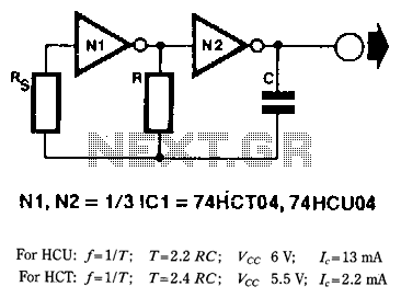
When frequency stability is not of primary importance, a simple yet reliable digital clock oscillator can be constructed using relatively few components. High-speed CMOS (HCU/HCf) inverters or gates with an inverter function are particularly suitable for creating such oscillators due to their low power consumption, good output signal definition, and wide frequency range. The circuit utilizes two inverters from a 74HCf04 or 74HCU04.
More: The basic design equations are as follows: For HCU: f ≈ 1/T; T ≈ 2.2RC; Vee = 6V; I ≈ 13mA. For HCT: f ≈ 1/T; T ≈ 2.4RC; Vee = 5.5V; I ≈ 2.2mA. With R1 and R2 calculated for a specific frequency and the value of C, both resistors can be implemented as presets to allow precise adjustment of the output frequency and the duty cycle. It is important to include small series resistors in series with the presets to observe the minimum values for R1 and R2, as indicated in the design equations. The specified values for current I are only applicable if the inputs of the remaining gates are grounded.
The digital clock oscillator circuit described utilizes high-speed CMOS inverters to achieve reliable oscillation characteristics. The choice of components, specifically the 74HCf04 or 74HCU04 series, ensures low power operation, making it an efficient solution for applications where frequency precision is not critical. The fundamental operation relies on the charging and discharging of a capacitor (C) through resistors (R1 and R2), which determine the oscillation frequency.
The frequency (f) of the oscillator is inversely related to the time period (T), which is derived from the resistor-capacitor (RC) time constant. The design equations indicate that for the HCU type, the time period is approximately 2.2 times the product of R and C, while for the HCT type, it is approximately 2.4 times the product of R and C. These equations provide the necessary relationships to calculate the values of R1 and R2 based on the desired output frequency.
To achieve precise frequency adjustment, the use of preset potentiometers for R1 and R2 is recommended. This allows for fine-tuning of the output frequency and duty cycle, which is essential in applications where timing accuracy is important, even if frequency stability is not the primary concern. Additionally, the inclusion of small series resistors is a critical design consideration to ensure that the resistors do not fall below their minimum operational values, which could adversely affect the circuit's performance.
In summary, the digital clock oscillator circuit is a straightforward design that leverages the advantages of high-speed CMOS technology to provide a reliable and adjustable frequency source for various electronic applications. The careful selection of components and adherence to design equations ensures the effectiveness of the oscillator in meeting the specified operational requirements.When frequency stability is not of prime importance, a simple, yet reliable, digital clock oscillator can be made with the aid of relatively few components. High-speed CMOS (HCU/HCf) inverters or gates with an inverter function are eminently suitable to make such oscillators, thanks to their low power consumption, good output signal definition, and extensive frequency range.
The circuit as shown uses two inverters in a 74HCf04 or 74HCU04. The basic design equations are: ForHCU: J~l!T; T~2.2RC; Vee 6V; I,~13mA For HCT: f~liT; T~2.4 RC; Vee 5.5 V; !,~2.2 mA With R, and R calculated for a given frequency and value of C, both resistors can be realized as presets to enable precise setting of the output frequency and the duty factor. Do not forget, however, to fit small series resistors in series with the presets, in obse=ce of the minimum values for R and R, as given in the design equations.
The values quoted for I, are only valid if the inputs of the remaining gates are grounded. 🔗 External reference