
High Power Full Bridge Flyback Driver circuit


The circuit utilizes the TL494 chip, a sophisticated pulse width modulation (PWM) control unit that includes two error amplifiers, an adjustable on-chip oscillator, a dead-time control comparator, a pulse-steering control flip-flop, a 5% precision regulator, and output-control circuits. The on-chip oscillator can be bypassed for external sawtooth inputs or used in synchronous multiple-rail power supplies. The architecture prevents simultaneous pulsing of either output during push-pull operation, allowing for selection between push-pull or single-ended output operation.
The second integrated circuit in the design is the TC4429, a high-speed MOSFET driver that operates at 6A. This inverting driver, fabricated in CMOS technology, offers lower power consumption and greater efficiency compared to bipolar drivers. It features TTL/CMOS compatible inputs that can handle voltages up to VDD + 0.3V or as low as -5V without damage. The rail-to-rail output swing provides a better drive voltage margin, particularly during power-up and power-down sequences. The TC4429 is designed to be virtually latch-up proof, functioning as an inverting MOSFET driver for half of the circuit to achieve full bridge action.
The circuit employs fifth-generation HEXFETs, specifically the IRFP250, known for their ultra-fast switching speeds and reliable operation. Four of these MOSFETs are used to achieve full bridge output, with two being driven by the TC4429 with inverted signals. Alternative MOSFET types can be utilized based on specific requirements.
Power Schottky barrier diodes are incorporated to withstand high switching currents at elevated speeds. Unlike standard silicon diodes, which exhibit a forward voltage drop of 600-700 mV, Schottky diodes have a forward voltage drop of 150-450 mV, enhancing switching speeds and system efficiency. The circuit utilizes the ESAD85-009 Schottky barrier diode, chosen for practical PCB design and heatsink placement considerations, although similar diodes can be substituted.
The PCB layout is designed for a single heatsink accommodating six components, compatible with commonly available heatsinks from old PCs. A 5-6mm hole should be drilled at the center of the heatsink for mounting on the PCB, ensuring proper heat dissipation from the MOSFETs and Schottky diodes. Insulating pads are necessary between components and the heatsink, especially under high power conditions. A small fan may be added above the heatsink if excessive heat is generated. The PCB express file is available for download.
Construction should commence with shorter components, using a medium-power soldering iron while adhering to the PCB layout. Care must be taken with the polarity and orientation of electrolytic capacitors, diodes, ICs, and MOSFETs. IC bases should be installed last to facilitate testing.
For operation, a regulated voltage supply of 15V is recommended, with a separate variable voltage and current supply for Vdd to maintain control over circuit operation. If correctly assembled, the circuit should function on the first power-up. If it does not, a component may be incorrectly connected. Any flyback transformer can be used, but those from old CRT TVs often contain internal high-voltage diodes or voltage multipliers, resulting in pulsed DC suitable for high-voltage free energy experiments. For AC output, a flyback transformer without an internal diode is required, or a custom-built flyback can be constructed. Multi-turn wirewound resistors should be used as potentiometers for improved precision, with a frequency range of 30-240 kHz.
Caution is advised when working with high voltage. Only individuals with appropriate technical education and experience should engage in high power or high voltage experiments. Respect for the dangers of high voltage is paramount, as it can be lethal.You need to find a reliable full bridge driver to drive your flyback transformer? Well, This is your final stop. There are many flyback drivers schematics out there, but most of them will not last for long. It is common known that famous ZVS invented by Vladmiro Mazilli, is the most reliable flyback driver as it uses the resonant zero voltage switching which result in less heat of the Mosfet's with large amount of current being used, and all that with just few electronic components. Usually in a driver/transformer system like that the weaker side most of the times is the transformer.
Most TV flyback transformers will by fried by the high current (so a current limiter is a must have when you play with ZVS). Another advantage beside the low heat and the high power of the ZVS is the fact that is a full bridge driver, which lets you experiments with AC projects too.
The disadvantage of ZVS is that there is not any frequency or duty-cycle dial. The frequency can be change only by varying the output capacitor. Something that is not so practical at all for most experimenters. Changing frequency is a must for people who experiment with resonant frequency or free energy experiments, resonant energy applications, tesla coils, etc. The circuit presented here is a very powerful full bridge driver with variable frequency and duty cycle.
It needs heatsinks offcourse if you want to play with high power. But its very precise, stable and durable.
The circuit
The circuit first of all uses the very well known TL494 chip witch is a pulse width modulation control unit designed in a very sophisticated way. It contains two error amplifiers, an on-chip adjustable oscillator, a dead-time control(DTC) comparator, a pulse-steering control flip-flop, 5%-precision regulator, and output-control circuits.
The on-chip oscillator can be bypassed by terminating RT to the reference output and providing a sawtooth input to CT, or it can drive the common circuits in synchronous multiple-rail power supplies.
The architecture of this device prohibits the possibility of either output being pulsed twice during push-pull operation. It provides for push-pull or single ended output operation, which can be selected through the output-control function.
The second IC chip that is being used as a MOSFET Driver and as inventer in the circuit is a 6A High Speed Mosfet Driver, the TC4429 by Microchip.
Its an inverting driver fabricated in CMOS for lower power and more efficient operation versus bipolar drivers. Its TTL/CMOS compatible inputs can be driven as high as VDD + 0.3V or as low as 5V without upset or damage to the device.
The output swing is rail-to-rail, ensuring better drive voltage margin, especially during power-up/power-down sequencing. Unlike other drivers, the TC4429 is virtually latch-up proof too. Here in circuit, it serves as an inverting mosfet driver for the half of the circuit the get the full bridge action.
The Mosfets that we use here are a fifth Generation HEXFETs IRFP250 with ultra fast switching speed and extremely efficient and reliable operation.
The circuit use four of those to achive full bridge output. Half of them are driven by the TC4429 with inverted signal. Offcourse you can use other type of Mosfet to fit your needs.
The circuit uses power schottky barrier diodes to stand the high switching currents at very high speeds. Why not a simple silicon diode? Because of a high current flows in the forward direction of 600-700 mV in a typical silicon diode, while the Schottky's forward voltage is 150-450 mV.
This lower forward voltage requirement allows higher switching speeds and better system efficiency. Here the ESAD85-009 schottky barrier diode is used for practical reasons in relation to PCB design and heatsink placement, but you can choose another similar type of schottky barrier diode with no problems.
PCB design and layout
The pcb is designed to have only one heatsink for 6 components.
Also it fit perfectly with a heatsink taken from an old PC. I am sure most of you can find this kind of heatsink which has more or less the same dimensions. the only thing that you have to do is to open a hole 5-6mm hole at the center of the heatsink for the screw to mount it on the PCB board. This screw also compress the heatsink to the Mosfets and schottky barrier diodes underneath it and spreads the heat perfectly.
Make sure you use insulating pads between all components and heatsink. If high power is being used and heat becomes a problem.You can use a small fan above the heatsink too. You can download the PCB express file at the end of the article.
Construction
Start from shorter in height components and up.
Use a medium power soldering iron and follow the PCB layout diagram. Just be careful with polarities and orientation of electrolytic capacitors, diodes, ICs, Mosfets, etc. The components under the heatsink have their "back" (metallic side) on top side of PCB, where the heatsink goes.
Use bases for both IC chips and place them at the end of construction, just before the first test.
operation and first run
Supply with regulated voltage Vcc 15V where the circuit shows. Use a separate power supply preferable a variable voltage and current supply at Vdd to have full control of the operation of the circuit.
Unlike other similar flyback drivers, this one, if everything is placed correctly on board, it will definitely run at the first power up. If not then definitely you have at least a component wrong connected. Check again and you will get it run for sure. The flyback transformer can be any.
Remember those from old CRT TVs have internal High Voltage diode and/or voltage multiplier and the result will be pulsed DC which is used in most high voltage free energy experiments, such as those of Tesla's, Don Smith's etc.
But again if you need AC output you must find a flyback transformer without internal diode, or you can build your own flyback if you have skills in building ;) Use multiturn wirewound resistors as potentiometers for better precision. Frequency range is 30-240KHz.
Caution
Be very careful with High Voltage. Only experienced and well technically educated people should experiment with high power/high Voltage experiments.
Respect the power and be reasonable. High Voltage is not game, its lethal !!
Related Circuits
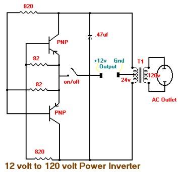
This is the schematic diagram of a 15W inverter circuit. The circuit is based on a PNP power transistor such as the TIP32 and other similar transistors. This inverter produces a square wave output, which may cause some noticeable...

Adjustment potentiometer RP can modify the conduction angle of thyristor Vl, vz, thus altering the voltage applied across the load Rfz. The adjustment potentiometer (RP) serves a critical role in controlling the conduction angle of the thyristors Vl and vz within...
The water tank overflow liquid level sensor alarm circuit is a straightforward electronics project suitable for school students. Previous discussions have covered numeric water level indicators and water level controller circuits, which are more complex and intended for engineering...

A 2x22 W car audio amplifier circuit utilizes the TDA1558, a monolithic integrated class-B output power amplifier that includes four 11 W single-ended amplifiers or two 22 W bridge-tied load (BTL) amplifiers. The TDA1558 is designed to drive speakers in...
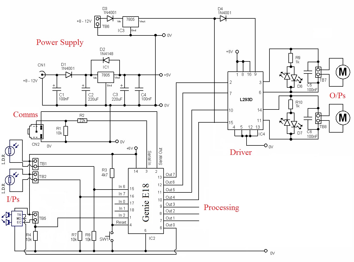
The circuit requires a power source to function. The PIC needs a 5-volt supply, while the driver demands a higher voltage to operate the motors. Inputs: The inputs come from three sensors. Two of these sensors are Light Dependent...
This circuit utilizes a single 555 Timer IC and a small transformer to generate high voltage for testing zener diodes with voltage ratings up to 50VDC. The 555 timer operates in astable mode, with the output at pin 3...