
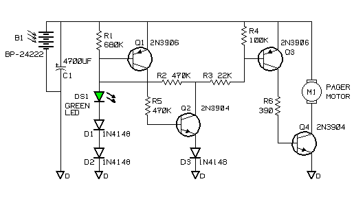
HIGH POWER SIREN
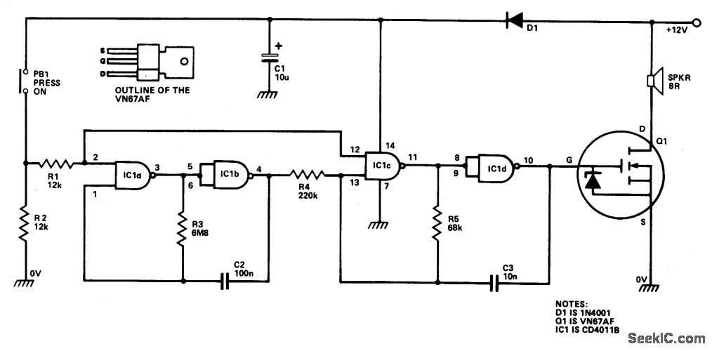
The circuit utilizes integrated circuits (ICs) configured in astable multivibrator arrangements to generate square wave signals at different frequencies. The slow astable multivibrator, comprising IC1a and IC1b, produces a lower frequency output. This output serves as a modulation signal for the fast astable multivibrator, which is implemented with IC1c and IC1d. The fast astable configuration generates a higher frequency signal that can be influenced by the modulation from the slow astable.
The gating mechanism, controlled by push button PB1, allows for the entire circuit to be turned on or off as needed. This feature is particularly useful in applications where power conservation is critical or where the circuit needs to be temporarily disabled without disconnecting power.
The output from the fast astable is fed to an external speaker through a VMOS (Vertical Metal Oxide Semiconductor) power FET amplifier stage, designated as Q1. This stage is responsible for amplifying the fast astable's output signal to a level suitable for driving the speaker. The use of a VMOS power FET is advantageous due to its high efficiency and ability to handle significant power levels, ensuring that the audio output is clear and loud enough for the intended application.
Overall, the described circuit provides a flexible and efficient means of generating audio signals with variable frequency modulation, suitable for various electronic applications, including sound synthesis or alert signaling systems.IC1a and IC1b are wired as a slow astable multivibrator and IC1c-IC1d are wired as a fast astable. Both are "gated" types, which can be turned on and off via PB1. The output of the slow astable modulates the frequency of the fast astable, and the output of the fast astable is fed to the external speaker via the Q1 VMOS power FET amplifier stage. 🔗 External reference
Related Circuits
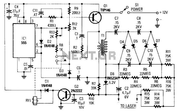
IC1 is a 555 timer operating at approximately 16 kHz. This integrated circuit drives Q1, a TIP146 transistor, which generates a 12-V square wave across the primary winding of transformer T1. This results in an output voltage ranging from...
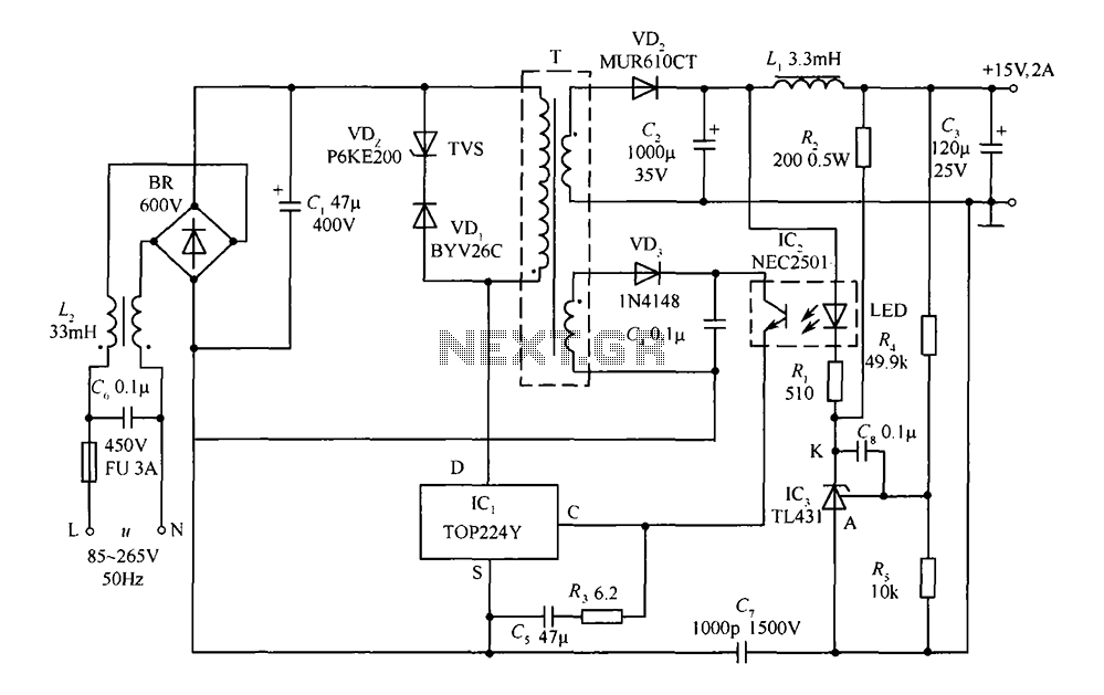
This circuit comprises a 15V TOP224Y, 2A output DC switching power supply. It utilizes three integrated circuits: IC1 is a monolithic regulator (TOP224Y), IC2 is an optocoupler (NEC2501), and IC3 is a precision voltage reference (TL431). The TL431 (IC3)...
This circuit utilizes a 74HC14 hex Schmitt trigger inverter as a square wave oscillator to drive a small signal transistor configured in a class C amplifier. The oscillator frequency can be set to a fixed value using a crystal...
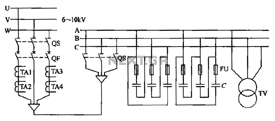
The compensation system is designed to focus on a high-pressure, high-voltage capacitor bank installed in the substation 6-10 kV bus. Compensation can only be implemented in this manner for the 6-10 kV bus before the reactive power on the...
A power source providing 2.5V DC at 10µA is utilized to drive a pager motor. The motor activates between 2.3V and 2.5V, and deactivates between 1.2V and 1.5V. The circuit design has been breadboarded by multiple individuals, showing consistent...
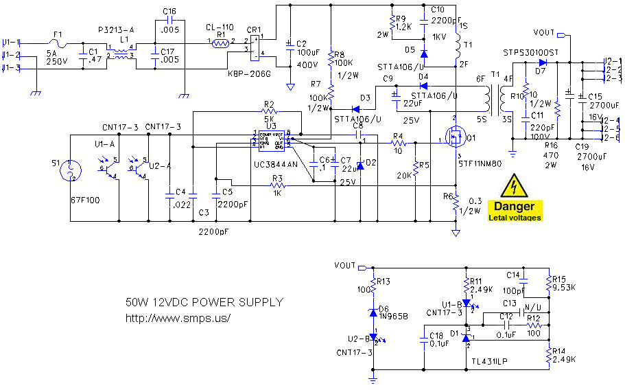
The schematic diagram below illustrates a simple and cost-effective 12-volt DC 50W off-line SMPS (switched-mode power supply) circuit. It is suitable for DIY home projects or for learning about the operation of flyback converters. This power supply unit (PSU)...