
High-voltage-bucking-regulator
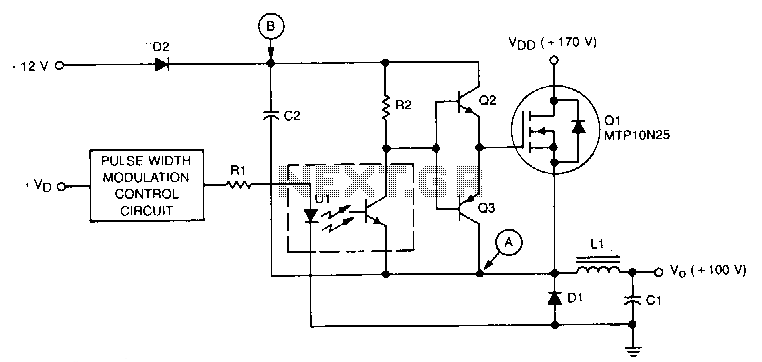
This circuit is essentially a classic buck regulator that utilizes a TMOS N-channel power FET for the chopper and generates its own supply for gate control. The unique feature of this circuit is its method for creating a separate supply for the gate circuit, which must exceed the voltage level Vvv. When power is applied, capacitor C2 charges through diode D2 to +12 V. At this point, transistor Q1 is off, and the voltage at point A is slightly below zero. When a pulse-modulated signal is applied, the optoisolator transistors Q2 and Q3 provide a signal to Q1, turning it on. The voltage at point A then rises to Vvn. Capacitor C2 back-biases diode D2, resulting in the voltage at point B becoming 12 V above Vnn. After Q1 is activated, current begins to flow through inductor L1 into capacitor C1, increasing until Q1 turns off. The current continues to flow through L1, causing the voltage at point A to drop towards negative infinity; however, it is clamped by diode D1 to just below zero. As current into C1 diminishes, Q1 turns on again. Transistors Q2 and Q3 drive Q1's gate between the voltages at points A and B, which consistently maintain a 12 V swing, ensuring that the maximum Vcs is not exceeded. For the circuit to function correctly, the 12 V supply must be established prior to the application of the pulse-width modulator signal.
This buck regulator circuit operates by stepping down a higher voltage to a lower voltage while maintaining high efficiency. The TMOS N-channel power FET, acting as the primary switching element, is responsible for controlling the flow of energy from the input source to the output load. The circuit's design incorporates feedback mechanisms through the use of optoisolators, which provide isolation and control for the gate of the power FET.
The charging of capacitor C2 through diode D2 is crucial for generating the necessary gate drive voltage. Once C2 reaches +12 V, it enables Q1 to switch on, allowing current to flow through L1. The inductor L1 plays a pivotal role in energy storage during the on-phase, and its inductance value is selected based on the desired output current and voltage ripple specifications.
As Q1 turns off, the energy stored in L1 must be managed to prevent excessive voltage spikes. Diode D1 clamps the voltage at point A, protecting the circuit from negative voltage excursions. The control strategy employed by the optoisolator transistors ensures that Q1 operates within safe limits, with the swing between points A and B providing a robust mechanism to regulate the output voltage.
Overall, this circuit exemplifies efficient power conversion using advanced semiconductor technology and careful design considerations to ensure reliability and performance in various applications.This circuit is basically tbe classic bucking regulator, except it uses a TMOS N-channel power FET for the chopper and creates its own supply for the gate control. Tht unique aspect of this circuit is how it generates a separate supply for the gate circuit, which must be greater than Vvv.
When power is applied, C2 charges, through D2, to +12 V. At this time, Q1 is off and the voltage at point A is just below zero. When the pulse-modulated signal is applied, the optoisolator transistors, Q2 and Q3, supply a signal to Q1 that turns it on. The voltage at point A then goes to Vvn. C2 back-biases D2, and the voltage at point B becomes 12 V above Vnn· After Q1 is turned on, current starts to flow through L1 into C1, increasing until Q1 turns off.
The current still wants to flow through Ll, so the voltage at point A moves toward negative infinity, but is clamped by D1 to just below zero. Current flows less and less into C1, until Q1 turns on again. Q2 and Q3 drive Q1 "s gate between the voltages at point A and B, which is always a12 V swing, so Vcs max.
is never exceeded. For proper operation, the 12-V supply has to be established before the pulse-width modulator signal is applied. 🔗 External reference