
how to design h bridge circuit for
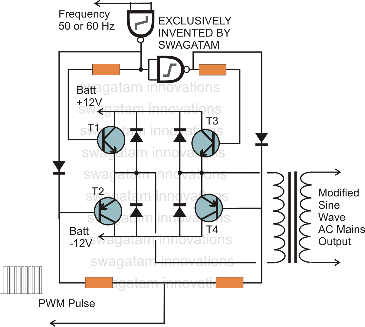
The H-bridge circuit is a crucial component in applications requiring bidirectional control of motors and other inductive loads. The four switches are typically arranged in a bridge topology, where two switches connect to the positive supply voltage and two connect to the ground. This configuration allows for the reversal of current through the load by selectively turning on the appropriate switches.
When designing an H-bridge, careful consideration must be given to the switching devices used, as they must handle the load current and voltage levels. MOSFETs are often preferred for their high efficiency and fast switching capabilities. Additionally, gate drivers may be employed to ensure that the transistors are turned on and off efficiently, minimizing switching losses and heat generation.
The control logic for the H-bridge can be implemented using microcontrollers or dedicated driver ICs, which provide the necessary PWM signals to modulate the output voltage and control the speed of the connected motor. The PWM frequency must be chosen based on the application requirements, balancing responsiveness and efficiency.
Protection features, such as diodes for flyback protection, should be incorporated to safeguard the circuit from voltage spikes generated by inductive loads. Furthermore, incorporating feedback mechanisms can enhance performance by allowing real-time adjustments to the PWM signals based on the load conditions.
In summary, the H-bridge circuit is a versatile and efficient solution for controlling the direction and speed of motors, making it an essential component in various electronic applications, including robotics, automotive systems, and industrial automation.In electronics H-bridge circuit refers to a configuration consisting of four individual switching devices like transistors or mosfets, such that these can be switched through external discrete signals from respective stages of the involved control circuit. While switching, the complementary pairs from each of the arms switch together, meaningthe NPN device from the left arm and the PNP
device from the right arm of the bridge conduct together in response to an external applied signal. The arrangement generates a push pull effect in the connected transformer winding of the inverter which in turn generates a required one full cycle of AC at the output of the transformer. The special arrangement of the devices make it possible for driving the devices through two individual signal sources, one which decides the switching rate of the output while the other decides the RMS value of the output from the transformer.
Transistors T2 and T4 ae fed with the PWM pulses which switch ON together, however when T1 is conducting, T2 should remain shut OFF and similarly when T3 conducts T4 should remain OFF, the two diodes from the respective NAND gates takes care of the issue and allow only the relevant transistors to carry out the PWM switching. Thus the NPN transistors are responsible for producing the regular 50 or 60 Hz pulses while the PNP transistors are responsible for breaking the square waves as per the PWM sections.
🔗 External reference
Related Circuits

This house alarm circuit features both open and closed loop sensors and includes a self-shutdown function. The delay after triggering can be adjusted between 1 minute and 12 minutes, while the delay before triggering is set at 13 seconds....
This page presents a replacement circuit for the LM3909 LED Flasher/Oscillator utilizing discrete components. The circuit functions similarly to the integrated LM3909 but features minor variations in the component values used. Although the LM3909 is still available, it tends...
The circuit diagram illustrates a portable solar charger that utilizes an LM358N operational amplifier and a single transistor. This regulator delivers a constant output of 2.4 volts DC, suitable for powering small devices requiring energy from two AA battery...

A circuit is needed to drive three or more LEDs at a current of 200-350mA each, with the capability to randomly flash or strobe them at a frequency of 5-20Hz. The input power should be low-voltage DC, with a...
The PowerSaver Flasher uses capacitive output coupling to produce brighter shorter flashes and has a much lower average current drain than standard bicore or 74HC14 flashers. The PS Flasher with one LED circuit (2 LEDs) runs all night from...
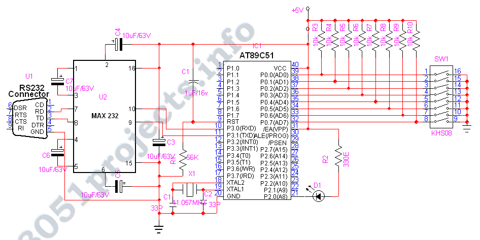
The 8051 microcontroller features a transmit channel and a receive channel for serial communication. The transmit data pin (TXD) is designated as P3.1, while the receive data pin (RXD) is located at P3.0. The serial signals on these pins...