
I2C Bus I2C Interface description
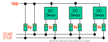
The I2C bus architecture is a popular choice for inter-device communication in embedded systems due to its simplicity and versatility. The two-wire configuration allows for efficient use of PCB space and minimizes wiring complexity. The pull-up resistors (Rp) are critical in ensuring that the SCL and SDA lines are maintained at a high logic level when not actively driven low by any device. The optional ESD protection resistor (Rs) enhances the robustness of the system, particularly in environments where devices may be hot-swapped.
In terms of data transmission, the half-duplex nature of I2C means that devices cannot send and receive data simultaneously, which is a trade-off for the simplicity of the two-wire interface. The acknowledgment mechanism is a vital part of the protocol, ensuring that data integrity is maintained. The Master device controls the timing of the communication and initiates data transfers, which is essential for coordinating the interactions between multiple devices on the bus.
The unique addressing scheme allows for a theoretically large number of devices on the bus, although practical limitations such as bus capacitance and physical layout must be considered. The maximum bus capacitance of 400pF effectively limits the number of devices that can be connected, and careful attention must be paid to the layout of the PCB or cable to maintain signal integrity.
In applications where devices operate at different voltage levels, I2C supports level translation, allowing seamless communication across devices with varying supply voltages. This feature enhances the flexibility of the I2C bus in mixed-voltage environments.
Overall, the I2C bus is an efficient and effective solution for communication in a wide range of electronic applications, from simple sensor networks to complex multi-device systems. Its ease of implementation and support for multiple devices make it a preferred choice for many designers in the field of electronics.The I2C bus uses a bi-directional Serial Clock Line [SCL] and Serial Data Lines [SDA]. Both the SCL and SDA lines are pulled high via an Rp resistor. Resistor Rs is optional, and used for ESD protection for `Hot-Swap` devices. No other lines are specified. Any device may be a Transmitter or Receiver, and a Master or Slave. Data and clock are sent from the Master ~ valid while the clock line is high. The link may have multiple Masters and Slaves on the bus, but only one Master may be active at any one time. I2C Slaves may receive or transmit data to the master. I2C, due to its two-wire nature (one clock, one data) can only communicate half-duplex. The maximum bus capacitance is 400pF, which sets the maximum number of devices on the I2C bus and the maximum line length.
The interface uses 8 bit long bytes, MSB [Most Significant Bit] first, with each device having a unique address. Data on the SDA data line only changes when the clock line [SCL] is low. However if SDA drops while SCL is high a start of frame is indicated. Also if SDA rises while SCL is high than a stop condition is indicated. The Start condition indicates a start of frame and the Stop condition indicates an end of frame. Each transfer on the I2C is 9 bits long, eight data bits followed by a `1` bit. The listener acknowledges the receipt of the byte in one of two ways; the listener may over write the `1` bit with a `0` bit indicating ready for more data.
or leaving the trailing `1` indicating not ready for data. The Master [talker] always generates the clock and the message. An I2C message begins with a Start bit, followed by a 7 bit Slave address and then a direction bit [`1` for Read, `0` for Write]. Once the slave address is sent, the slave is required to respond, otherwise the master will send a Stop or Retry bit.
If the Master sends a Write bit, the master will follow that with a sub-address to indicate a particular register. The slave will stop acknowledging the last byte of the transfer. Remember that the I2C bus is defined as having a maximum capacitance of 400pF, that defines the maximum number of I2C components on the I2C bus and the I2C length [in combination].
So the I2C Bus length is never defined in the I2C Bus specification. However, there is one note in the interface specification: If the length of the bus lines on a PCB or ribbon cable exceeds 10 cm and includes the VDD and VSS lines, the wiring pattern must be: SDA - [Power/Ground or Ground] - SCL, or no Vdd/Vss lines if there embedded within the PCB. Of course this could also be a twisted pair or shielded cable but I2C cable length still depends on the type of cable [and its capacitance] and the number of I2C devices.
The voltage VDD may be different for each device, but all devices have to relate their output levels to the voltage produced by the pull-up resistors [RP] It is possible to run off two different bus voltages, but they have to be translated [refer to the spec. ]. The I2C serial interface above show the I2C Pull-Up connecting to Vdd [supply voltage]. The I2C bus may also be seen as the Inter-IC Bus or the IIC Bus which all mean the same thing. The most common term is of course I2C. Of course there are always other references; I2C Serial Port, I2C Digital Interface, I2C Interface or I2C Interface Specification.
🔗 External reference
Related Circuits
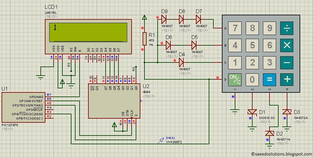
This post provides a simple method to interface any keypad (e.g., 4x4 or 4x3) with the PIC12F675 microcontroller. The code for the PIC12F675 is written in C language. The interfacing of a keypad with the PIC12F675 microcontroller involves several key...
Many applications require a large number of keys connected to a computing system. Examples include PC keyboards, cell phone keypads, and calculators. Connecting a single key to a microcontroller unit (MCU) is straightforward; however, connecting 10 or 100 keys...
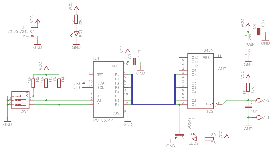
The board is relatively simple and is based on a PCF8574, which provides the output of a CD 4040 counter to the I2C bus. A DIP switch is included to select the PCF8574 address, along with some LEDs for...
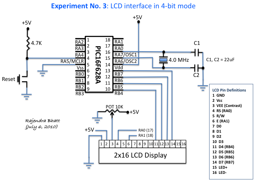
An HD44780 Character LCD is a liquid crystal display (LCD) device designed for interfacing with embedded systems. These screens are available in various configurations, including 8x1 (one row of eight characters), 16x2, and 20x4. The most commonly produced configuration...
The yellow wires on the far right serve as temporary power connections, allowing battery power to enter through the contact studs located in the large holes that press against the radio's battery terminals. The cable in the lower right...
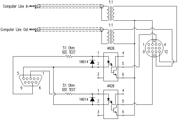
This document outlines a modification that connects a radio to a computer. It is important to proceed with caution and recognize that the responsibility for any consequences lies with the user. The design has been tested on an Icom...