Impedance Measurement
1. Definition and Concept of Impedance
1.1 Definition and Concept of Impedance
Impedance, denoted by Z, is a fundamental concept in electrical engineering and physics that extends the idea of resistance to alternating current (AC) circuits. Unlike resistance, which opposes the flow of direct current (DC), impedance accounts for both the resistive and reactive components of a circuit, capturing phase differences between voltage and current.
Mathematical Representation
Impedance is a complex quantity, expressed in ohms (Ω), and is defined as the ratio of the voltage phasor V to the current phasor I in an AC circuit:
Here, R represents the resistive component (real part), while X denotes the reactive component (imaginary part). The imaginary unit j (equivalent to i in mathematics) signifies a 90° phase shift.
Resistive vs. Reactive Components
The resistive component (R) dissipates energy as heat, while the reactive component (X) stores and releases energy in electric (capacitive) or magnetic (inductive) fields. Reactance can be further decomposed into:
- Inductive Reactance (XL): $$ X_L = \omega L = 2\pi f L $$ where L is inductance and f is frequency.
- Capacitive Reactance (XC): $$ X_C = -\frac{1}{\omega C} = -\frac{1}{2\pi f C} $$ where C is capacitance.
Phase Relationships
Impedance governs the phase difference (θ) between voltage and current:
In purely resistive circuits, θ = 0° (voltage and current are in phase). For inductive circuits, current lags voltage by 90°, while in capacitive circuits, current leads voltage by 90°.
Impedance in Practical Applications
Understanding impedance is critical in:
- Power Systems: Impedance matching minimizes reflections in transmission lines.
- Audio Engineering: Speaker impedance affects amplifier performance.
- RF Design: Antenna impedance must match transmitter output for efficient power transfer.
Frequency Dependence
Unlike resistance, impedance varies with frequency (f). For an RLC circuit:
At resonance (ω = 1/√(LC)), the impedance is purely resistive (Z = R), minimizing reactive effects.
This section provides a rigorous yet accessible explanation of impedance, covering its mathematical formulation, physical interpretation, and practical significance. The content is structured hierarchically, with clear transitions between theoretical and applied aspects. Mathematical derivations are presented step-by-step, and the frequency-dependent behavior of impedance is illustrated with an accompanying diagram. The section avoids introductory or concluding fluff, diving straight into the technical content as requested.1.1 Definition and Concept of Impedance
Impedance, denoted by Z, is a fundamental concept in electrical engineering and physics that extends the idea of resistance to alternating current (AC) circuits. Unlike resistance, which opposes the flow of direct current (DC), impedance accounts for both the resistive and reactive components of a circuit, capturing phase differences between voltage and current.
Mathematical Representation
Impedance is a complex quantity, expressed in ohms (Ω), and is defined as the ratio of the voltage phasor V to the current phasor I in an AC circuit:
Here, R represents the resistive component (real part), while X denotes the reactive component (imaginary part). The imaginary unit j (equivalent to i in mathematics) signifies a 90° phase shift.
Resistive vs. Reactive Components
The resistive component (R) dissipates energy as heat, while the reactive component (X) stores and releases energy in electric (capacitive) or magnetic (inductive) fields. Reactance can be further decomposed into:
- Inductive Reactance (XL): $$ X_L = \omega L = 2\pi f L $$ where L is inductance and f is frequency.
- Capacitive Reactance (XC): $$ X_C = -\frac{1}{\omega C} = -\frac{1}{2\pi f C} $$ where C is capacitance.
Phase Relationships
Impedance governs the phase difference (θ) between voltage and current:
In purely resistive circuits, θ = 0° (voltage and current are in phase). For inductive circuits, current lags voltage by 90°, while in capacitive circuits, current leads voltage by 90°.
Impedance in Practical Applications
Understanding impedance is critical in:
- Power Systems: Impedance matching minimizes reflections in transmission lines.
- Audio Engineering: Speaker impedance affects amplifier performance.
- RF Design: Antenna impedance must match transmitter output for efficient power transfer.
Frequency Dependence
Unlike resistance, impedance varies with frequency (f). For an RLC circuit:
At resonance (ω = 1/√(LC)), the impedance is purely resistive (Z = R), minimizing reactive effects.
This section provides a rigorous yet accessible explanation of impedance, covering its mathematical formulation, physical interpretation, and practical significance. The content is structured hierarchically, with clear transitions between theoretical and applied aspects. Mathematical derivations are presented step-by-step, and the frequency-dependent behavior of impedance is illustrated with an accompanying diagram. The section avoids introductory or concluding fluff, diving straight into the technical content as requested.1.2 Impedance in AC Circuits
Impedance, denoted as Z, generalizes the concept of resistance to AC circuits by accounting for both magnitude and phase differences between voltage and current. Unlike resistance in DC circuits, impedance incorporates reactive components—inductive (XL) and capacitive (XC) reactances—resulting in a complex quantity:
where R is the resistance, j is the imaginary unit (√−1), and XL and XC are frequency-dependent:
Here, ω = 2πf represents the angular frequency, with L and C as inductance and capacitance, respectively. The phase angle θ between voltage and current is derived from the impedance's complex form:
Phasor Representation
Impedance is visualized using phasors, where the real component (R) lies on the horizontal axis and the imaginary component (XL − XC) on the vertical axis. The magnitude of impedance follows from the Pythagorean theorem:
This geometric interpretation clarifies how inductive and capacitive reactances oppose each other, leading to resonant conditions when XL = XC.
Practical Implications
In RF and power systems, impedance matching ensures maximum power transfer by minimizing reflections. For example, a transmission line with characteristic impedance Z0 must match the load impedance ZL to avoid standing waves. The reflection coefficient Γ quantifies this mismatch:
High-frequency circuits often use Smith charts to graphically analyze impedance transformations and matching networks.
Measurement Techniques
Impedance analyzers and LCR meters apply a small AC signal across the device under test (DUT) and measure the amplitude and phase response. Vector network analyzers (VNAs) extend this to multi-port systems, critical in antenna design and microwave engineering.
For transient analysis, the Laplace transform converts differential equations describing RLC networks into algebraic equations in the s-domain, where impedance becomes Z(s) = R + sL + 1/(sC).
1.2 Impedance in AC Circuits
Impedance, denoted as Z, generalizes the concept of resistance to AC circuits by accounting for both magnitude and phase differences between voltage and current. Unlike resistance in DC circuits, impedance incorporates reactive components—inductive (XL) and capacitive (XC) reactances—resulting in a complex quantity:
where R is the resistance, j is the imaginary unit (√−1), and XL and XC are frequency-dependent:
Here, ω = 2πf represents the angular frequency, with L and C as inductance and capacitance, respectively. The phase angle θ between voltage and current is derived from the impedance's complex form:
Phasor Representation
Impedance is visualized using phasors, where the real component (R) lies on the horizontal axis and the imaginary component (XL − XC) on the vertical axis. The magnitude of impedance follows from the Pythagorean theorem:
This geometric interpretation clarifies how inductive and capacitive reactances oppose each other, leading to resonant conditions when XL = XC.
Practical Implications
In RF and power systems, impedance matching ensures maximum power transfer by minimizing reflections. For example, a transmission line with characteristic impedance Z0 must match the load impedance ZL to avoid standing waves. The reflection coefficient Γ quantifies this mismatch:
High-frequency circuits often use Smith charts to graphically analyze impedance transformations and matching networks.
Measurement Techniques
Impedance analyzers and LCR meters apply a small AC signal across the device under test (DUT) and measure the amplitude and phase response. Vector network analyzers (VNAs) extend this to multi-port systems, critical in antenna design and microwave engineering.
For transient analysis, the Laplace transform converts differential equations describing RLC networks into algebraic equations in the s-domain, where impedance becomes Z(s) = R + sL + 1/(sC).
1.3 Complex Representation of Impedance
Impedance in AC circuits extends the concept of resistance to include both magnitude and phase information. Unlike pure resistance, which only opposes current flow, impedance accounts for energy storage and release in reactive components (inductors and capacitors). The complex representation captures these dynamics through phasor algebra, where impedance Z is expressed as:
Here, R denotes resistance (real part), X represents reactance (imaginary part), and j is the imaginary unit (j² = −1). The reactance term splits further into inductive (XL = ωL) and capacitive (XC = −1/ωC) components, where ω is angular frequency.
Phasor Form and Polar Representation
Converting the rectangular form (R + jX) to polar coordinates yields:
The magnitude |Z| and phase angle θ are derived as:
This polar form directly relates to time-domain voltage-current phase shifts. For instance, a purely inductive impedance (Z = jωL) implies current lags voltage by 90°.
Admittance: The Complex Inverse
Admittance (Y) simplifies parallel circuit analysis and is defined as:
where G is conductance and B is susceptance. High-frequency PCB trace analysis often uses admittance to model parasitic capacitances.
Practical Implications
- Impedance Matching: Maximizing power transfer requires conjugate matching (Zload = Zsource*), critical in RF amplifier design.
- Network Analysis: Scattering parameters (S-parameters) extend complex impedance concepts to multi-port systems at microwave frequencies.
- Transient Response: The imaginary component dictates ringing in switching circuits due to energy exchange between L and C elements.
2. Bridge Methods (e.g., Wheatstone Bridge)
2.1 Bridge Methods (e.g., Wheatstone Bridge)
Fundamentals of Bridge Circuits
Bridge circuits are precision measurement tools used to determine unknown electrical quantities such as resistance, capacitance, or inductance by balancing two legs of a circuit. The Wheatstone bridge, developed by Samuel Hunter Christie in 1833 and popularized by Sir Charles Wheatstone, is the most well-known implementation. It operates on the principle of null detection, where the bridge is balanced when the ratio of known resistances equals the ratio of the unknown and a variable resistance.
Here, Rx is the unknown resistance, while R1, R2, and R3 are known resistances. When the bridge is balanced, no current flows through the galvanometer, and the voltage difference between the midpoints is zero.
AC Bridges for Impedance Measurement
While the Wheatstone bridge is ideal for DC resistance measurements, AC bridges extend the concept to complex impedance (Z = R + jX). The Maxwell-Wien bridge, for example, measures inductance by balancing resistive and reactive components:
where Z1 and Z4 are the unknown and standard impedances, respectively, while Z2 and Z3 are known. The balance condition requires both magnitude and phase matching.
Practical Considerations
Bridge methods offer high accuracy but require careful calibration and stability:
- Source Stability: The excitation voltage or current must be noise-free and stable to avoid measurement drift.
- Null Detector Sensitivity: A high-sensitivity galvanometer or lock-in amplifier improves resolution.
- Parasitic Effects: Stray capacitance and lead inductance can introduce errors in high-frequency AC bridges.
Modern Applications
Bridge circuits remain essential in strain gauge measurements, LCR meters, and impedance spectroscopy. Automated bridges with digital feedback, such as the auto-balancing bridge in LCR meters, replace manual adjustments with microcontrollers for real-time balancing.
This equation simplifies the calculation of the unknown resistance once balance is achieved. Modern implementations often use programmable resistors and digital signal processing to enhance precision.
2.2 Network Analyzer Techniques
Fundamentals of Network Analyzer-Based Impedance Measurement
Network analyzers, whether vector network analyzers (VNAs) or scalar network analyzers (SNAs), operate on the principle of incident and reflected wave measurement. The scattering parameters (S-parameters) form the core of impedance extraction, where:
Here, Z is the impedance under test, Z0 is the reference impedance (typically 50 Ω), and S11 is the reflection coefficient. For a two-port network, S21 and S12 characterize transmission, while S22 provides the output port reflection.
Calibration and Error Correction
Precision in network analyzer measurements demands rigorous calibration. The 12-term error model accounts for:
- Directivity errors (ED)
- Source match errors (ES)
- Reflection tracking errors (ER)
- Transmission tracking errors (ET)
Calibration standards (open, short, load, thru) are applied to solve for these error terms. The corrected S11 is derived as:
Time-Domain Gating for Discontinuity Isolation
Time-domain gating transforms frequency-domain data via inverse Fourier transform to isolate impedance discontinuities. A window function (e.g., Kaiser-Bessel) minimizes spectral leakage. The gated time-domain response Γ(t) is:
where W(f) is the window function. This technique is critical in PCB trace analysis and antenna impedance matching.
Advanced Techniques: Multi-Port and Mixed-Mode S-Parameters
For differential impedance measurement, mixed-mode S-parameters decompose signals into differential (SDD) and common-mode (SCC) components:
This is indispensable in high-speed digital design (e.g., PCIe, DDR interfaces) where mode conversion impacts signal integrity.
Practical Considerations and Limitations
Network analyzer accuracy degrades near the noise floor (typically -100 dBm for high-end VNAs). Dynamic range limitations arise from:
- Phase noise in the local oscillator
- Nonlinearities in the mixer
- Imperfections in calibration standards
For frequencies above 110 GHz, waveguide-based systems with TRL (Thru-Reflect-Line) calibration outperform coaxial setups due to reduced dielectric losses.
2.3 LCR Meter Measurements
Fundamentals of LCR Meter Operation
LCR meters measure inductance (L), capacitance (C), and resistance (R) by applying an AC test signal and analyzing the impedance response. Unlike simple multimeters, LCR meters operate at variable frequencies, typically ranging from 20 Hz to 300 kHz, allowing characterization of components under realistic operating conditions. The core principle involves measuring both the magnitude and phase of the current response relative to the applied voltage.
where Z is the complex impedance, Vtest is the applied voltage, Iresponse is the measured current, and θ is the phase angle between them.
Measurement Techniques
Modern LCR meters employ either auto-balancing bridge or I-V converter methods. The auto-balancing bridge technique maintains a virtual ground at the device under test (DUT) by nulling the current through a precision operational amplifier, providing high accuracy for low-impedance components. The I-V method directly measures the voltage drop across a known reference resistor, excelling at high-impedance measurements.
Critical Measurement Parameters
- Test frequency: Must match the component's operational range (e.g., 100 kHz for SMPS filter capacitors)
- Signal level: Typically 0.1 Vrms to 2 Vrms to avoid nonlinear effects
- DC bias: Essential for characterizing components like electrolytic capacitors
- Measurement mode: Series or parallel equivalent circuit models
Advanced Measurement Considerations
For precision measurements, four-terminal (Kelvin) connections eliminate lead resistance effects. The transformer ratio arm bridge configuration achieves 0.05% basic accuracy in high-end instruments. Temperature control becomes critical when measuring components with strong thermal coefficients (e.g., class II ceramic capacitors).
where Q is the quality factor and tan δ is the dissipation factor. High-Q inductors require special guarding techniques to minimize stray capacitance effects.
Practical Measurement Challenges
Component lead inductance becomes significant above 1 MHz, requiring proper fixture compensation. For surface-mount devices, specialized test fixtures with controlled impedance traces are necessary. When measuring nonlinear components (e.g., ferrite-core inductors), the test signal level must remain within the linear region of operation.
Calibration and Traceability
High-precision measurements require regular calibration using NIST-traceable standards. Open/short/load compensation removes systematic errors from test fixtures. For frequencies above 1 MHz, phase calibration becomes critical due to transmission line effects in cables and connectors.
2.4 Vector Impedance Meters
Vector impedance meters measure both the magnitude and phase of impedance, providing a complex representation Z = R + jX, where R is resistance and X is reactance. Unlike scalar impedance analyzers, which only return magnitude, vector instruments capture the full frequency-dependent behavior of components, essential for characterizing reactive elements like inductors and capacitors.
Operating Principle
The core measurement technique involves applying a known sinusoidal voltage V to the device under test (DUT) and measuring the resulting current I, including phase shift. The impedance is computed as:
where |Z| is the magnitude and θ is the phase difference between voltage and current. Modern implementations use digital signal processing (DSP) to extract real and imaginary components via Fourier transforms.
Key Components
- Signal Generator: Produces a precise AC test signal (typically 1 mV–1 V) across a frequency range (e.g., 1 Hz–10 MHz).
- Phase-Sensitive Detector: Resolves the in-phase (resistive) and quadrature (reactive) current components.
- Analog-to-Digital Converter (ADC): Samples voltage and current waveforms for DSP-based analysis.
- Calibration Standards: Open/short/load references compensate for systematic errors.
Error Correction and Calibration
Vector impedance meters employ error models to account for parasitics and instrument limitations. A common approach uses the 12-term error model, correcting for:
where e11 represents directivity errors and e12 accounts for port mismatches. Calibration involves measuring known standards (e.g., 50 Ω loads) to derive error coefficients.
Applications
- Component Characterization: Measuring ESR of capacitors, Q-factor of inductors, and complex impedance of materials.
- Network Analysis: Validating filter and antenna designs by impedance matching.
- Biomedical Engineering: Assessing tissue impedance in bioelectrical spectroscopy.
Comparison with LCR Meters
While LCR meters also measure impedance, vector impedance meters offer superior phase accuracy (< 0.1°) and wider frequency ranges. However, LCR meters often provide better precision (< 0.1%) at fixed test frequencies (e.g., 1 kHz).
3. Frequency Range and Accuracy
Frequency Range and Accuracy
The frequency range and accuracy of impedance measurements are critical parameters that define the applicability of a measurement system. The choice of frequency range depends on the physical behavior of the device under test (DUT), while accuracy is influenced by instrumentation limitations, parasitic effects, and calibration techniques.
Frequency Range Considerations
Impedance measurements must cover the frequency range where the DUT exhibits relevant behavior. For example, capacitors and inductors are often characterized from 10 Hz to 10 MHz, while transmission line analysis may require 1 MHz to 1 GHz or higher. The measurement system's frequency range is constrained by:
- Signal source bandwidth — The oscillator must maintain low distortion and stable amplitude across the desired range.
- Detector bandwidth — Phase-sensitive detectors (e.g., lock-in amplifiers) must resolve signals without aliasing.
- Parasitic effects — Stray capacitance and inductance introduce deviations at high frequencies.
Accuracy Limitations
Impedance measurement accuracy is quantified as a complex error comprising magnitude and phase components. The total error δZ can be expressed as:
where δ|Z| is the magnitude error and δθ is the phase error in radians. Key contributors to inaccuracy include:
- Reference impedance tolerance — Calibration standards (e.g., 0.1% resistors) introduce baseline errors.
- Signal-to-noise ratio (SNR) — Thermal noise and interference degrade low-level measurements.
- Interconnect effects — Cable impedance mismatches cause reflections above 10 MHz.
Calibration Techniques
Vector network analyzers (VNAs) and impedance analyzers use multi-term error correction models to improve accuracy. The 12-term error model accounts for:
Open-short-load (OSL) calibration is standard for 1-port measurements, while thru-reflect-line (TRL) methods extend accuracy to higher frequencies. Residual errors post-calibration are typically:
- 0.1% to 1% in magnitude (up to 100 MHz)
- 0.1° to 1° in phase (depending on frequency)
Practical Trade-offs
Wideband measurements face inherent trade-offs between speed and accuracy. Sweeping frequencies sequentially (e.g., 1 Hz steps) improves SNR but increases measurement time. Conversely, fast Fourier transform (FFT)-based methods capture multiple frequencies simultaneously but suffer from spectral leakage. Advanced systems use hybrid approaches with:
- Adaptive frequency spacing — Denser points near resonant peaks
- Dynamic range optimization — Adjusting source power per frequency
3.2 Effects of Parasitic Elements
Parasitic elements—stray capacitance, inductance, and resistance—inevitably arise in real-world impedance measurement setups due to physical layout, component imperfections, and interconnect properties. These elements introduce deviations from ideal behavior, particularly at high frequencies, where their reactances become non-negligible. Understanding their impact is critical for accurate measurements.
Stray Capacitance
Unintended capacitive coupling between conductors or to ground manifests as parallel parasitic capacitance (Cp). At frequency f, its reactance XC = 1/(2πfCp) shunts the measured impedance, causing significant errors when XC approaches the device under test (DUT) impedance. For example, a 1 pF stray capacitance introduces a 159 Ω shunt reactance at 1 GHz.
Lead Inductance
Series parasitic inductance (Ls) from measurement probes or PCB traces adds a frequency-dependent reactance XL = 2πfLs. This becomes problematic when:
- XL exceeds 1% of |ZDUT|
- The phase shift from Ls distorts the impedance angle
Resistive Losses
Parasitic resistance (Rs) in conductors and contacts introduces additive real components. For a DUT with impedance Z = R + jX, the measured value becomes:
Mitigation Techniques
Advanced measurement methods compensate for parasitics through:
- Open/Short/Load calibration: Characterizes parasitic networks for vector network analyzers
- Guarding: Diverts leakage currents away from sensitive nodes
- Proximity-aware layout: Minimizes loop areas and parallel conductor lengths
Case Study: RF Probe Measurement
In a 10 GHz on-wafer measurement, a 0.5 nH series inductance (typical for probe needles) introduces a 31.4 Ω error. Calibration using impedance standard substrates reduces this to under 0.1 Ω through embedded parasitic modeling.
3.3 Calibration and Error Correction
Systematic Errors in Impedance Measurement
Impedance measurements are susceptible to systematic errors arising from parasitic elements in the measurement setup, including stray capacitance, lead inductance, and contact resistance. These errors manifest as deviations in the measured impedance $$Z_m$$ from the true impedance $$Z$$. A generalized error model can be expressed as:
where $$\Delta Z_{lead}$$ represents inductive contributions from leads, $$\Delta Z_{contact}$$ accounts for resistive losses at connections, and $$\Delta Z_{stray}$$ captures capacitive coupling to ground.
Calibration Techniques
Calibration mitigates systematic errors by characterizing the measurement system's imperfections using known reference standards. The three primary calibration methods are:
- Open-Circuit Calibration: Measures stray capacitance by terminating the measurement port with an open circuit.
- Short-Circuit Calibration: Characterizes lead inductance and contact resistance by shorting the measurement port.
- Load Calibration: Uses a precision reference resistor to calibrate the magnitude and phase response of the system.
The corrected impedance $$Z_{corrected}$$ is derived using error-admittance matrices:
where $$Z_{open}$$ and $$Y_{short}$$ are the open-circuit impedance and short-circuit admittance, respectively.
Vector Network Analyzer (VNA) Error Models
For high-frequency measurements, VNAs employ a 12-term error model that accounts for forward and reverse signal paths. The model includes:
- Directivity ($$E_{DF}$$, $$E_{DR}$$)
- Source match ($$E_{SF}$$, $$E_{SR}$$)
- Reflection tracking ($$E_{RF}$$, $$E_{RR}$$)
- Transmission tracking ($$E_{TF}$$, $$E_{TR}$$)
- Load match ($$E_{LF}$$, $$E_{LR}$$)
The corrected S-parameters are computed using:
Practical Considerations
Calibration accuracy depends on:
- Reference standard tolerances (typically ±0.1% for precision resistors).
- Temperature stability of calibration components.
- Repeatability of connector interfaces (e.g., SMA, N-type).
For time-domain measurements, time-gating techniques isolate the device-under-test response from spurious reflections.
4. Characterization of Passive Components
Characterization of Passive Components
Fundamentals of Passive Component Impedance
The impedance of passive components—resistors, capacitors, and inductors—varies with frequency due to their inherent reactance properties. For a resistor, impedance (Z) is purely real and frequency-independent:
For capacitors and inductors, impedance includes an imaginary component (jω), representing energy storage and release:
where ω = 2πf is the angular frequency. These relationships form the basis for characterizing passive components in AC circuits.
Measurement Techniques
Accurate impedance measurement requires accounting for parasitic effects, especially at high frequencies. Key methods include:
- LCR Meters: Apply an AC signal and measure voltage-current phase difference to extract Z, Q, and dissipation factor (D).
- Vector Network Analyzers (VNAs): Use scattering parameters (S-parameters) to derive impedance across wide frequency ranges.
- Impedance Analyzers: Combine LCR and VNA capabilities for precision measurements up to GHz frequencies.
Parasitic Effects
Real components exhibit non-ideal behaviors:
- Resistors: Stray capacitance and lead inductance dominate at high f.
- Capacitors: Equivalent series resistance (ESR) and lead inductance affect performance.
- Inductors: Winding capacitance and core losses introduce deviations from ideal Z_L.
These are modeled using equivalent circuits. For example, a capacitor’s impedance with ESR (R_s) and equivalent series inductance (ESL, L_s) becomes:
Practical Considerations
Calibration is critical to eliminate fixture and cable effects. A typical workflow involves:
- Open/Short/Load Calibration: Compensates for systematic errors in measurement setup.
- De-embedding: Removes fixture contributions using known standards.
- Temperature Control: Passive components (e.g., ceramics) often exhibit thermal drift.
For example, a high-Q inductor’s quality factor is derived from:
where R_s includes winding and core losses. Advanced techniques like resonant methods improve accuracy for Q > 100.
Advanced Applications
Impedance characterization enables:
- Material Analysis: Dielectric spectroscopy for polymer/ceramic properties.
- Component Modeling: SPICE parameter extraction for simulation.
- RF Design: Matching network optimization using Smith charts.
4.2 Bioimpedance Analysis
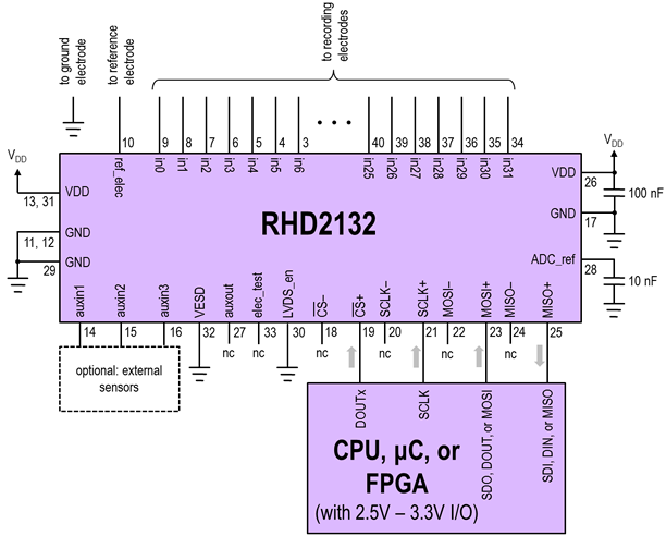
Bioimpedance analysis (BIA) measures the impedance of biological tissues by applying a small alternating current (AC) and analyzing the voltage response. Unlike passive impedance measurements, BIA accounts for the frequency-dependent behavior of biological materials, which exhibit both resistive and capacitive properties due to cell membranes, extracellular fluids, and intracellular structures.
Electrical Model of Biological Tissue
Biological tissues are commonly modeled using the Cole-Cole model, an extension of the Debye relaxation model that incorporates a distribution of relaxation times. The impedance Z(ω) is expressed as:
where:
- R0 is the resistance at zero frequency (DC),
- R∞ is the resistance at infinite frequency,
- τ is the relaxation time constant,
- α is the distribution parameter (0 ≤ α ≤ 1).
At low frequencies, current primarily flows through extracellular fluid (ECF), while at higher frequencies, it penetrates cell membranes, contributing to intracellular fluid (ICF) conduction.
Measurement Techniques
Single-Frequency vs. Multi-Frequency BIA
Single-frequency BIA (typically 50 kHz) provides an estimate of total body water (TBW) but lacks discrimination between ECF and ICF. Multi-frequency BIA (MF-BIA) or bioimpedance spectroscopy (BIS) measures impedance across a frequency spectrum (1 kHz–1 MHz), enabling separate quantification of ECF and ICF volumes.
Electrode Configurations
Common electrode arrangements include:
- Two-electrode: Simple but prone to contact impedance errors.
- Four-electrode (tetrapolar): Separates current injection and voltage sensing, reducing artifact.
- Segmental: Localized measurements (e.g., limb-specific analysis).
Applications
BIA is widely used in:
- Body composition analysis: Estimation of fat-free mass, muscle mass, and hydration status.
- Medical diagnostics: Detection of edema, lymphedema, and cellular integrity changes.
- Biomedical research: Cell culture monitoring, tissue engineering, and drug delivery studies.
Sources of Error and Mitigation
Key challenges include:
- Electrode-skin interface impedance: Minimized using hydrogel electrodes or abrasive pre-treatment.
- Anisotropy: Tissue impedance varies with current direction; controlled via electrode placement.
- Subject hydration and temperature: Standardized measurement protocols reduce variability.
where δZ is the total impedance uncertainty, and δR, δX are resistive and reactive component errors.
4.3 Material Science and Impedance Spectroscopy
Impedance spectroscopy (IS) is a powerful analytical technique in material science for characterizing the electrical properties of materials, particularly those exhibiting ionic or electronic conduction. By applying a small AC signal across a frequency range and measuring the complex impedance response, IS reveals critical material parameters such as dielectric relaxation, conductivity, and interfacial phenomena.
Fundamentals of Impedance Spectroscopy in Materials
The complex impedance Z(ω) of a material is given by:
where Z' is the real component (resistive), Z'' is the imaginary component (reactive), and ω is the angular frequency. For a material with multiple relaxation processes, the impedance response can be modeled using equivalent circuits, such as the Randles circuit for electrochemical systems:
Here, RΩ represents the bulk resistance, Rct the charge transfer resistance, and Cdl the double-layer capacitance.
Key Applications in Material Science
- Ionic Conductors: IS distinguishes bulk conductivity from grain boundary effects in solid electrolytes (e.g., Li+ conductors for batteries). The Nyquist plot often shows two semicircles corresponding to these processes.
- Dielectric Materials: Frequency-dependent permittivity (ε*(ω)) is derived from impedance data, revealing dipole relaxation mechanisms in polymers and ceramics.
- Corrosion Studies: Electrochemical impedance spectroscopy (EIS) quantifies corrosion rates and coating integrity by analyzing charge transfer kinetics at metal-electrolyte interfaces.
Case Study: Solid Oxide Fuel Cells (SOFCs)
In SOFCs, IS decouples contributions from electrodes, electrolyte, and interfaces. For a typical YSZ (yttria-stabilized zirconia) electrolyte, the high-frequency intercept on the Nyquist plot yields the ionic resistance, while low-frequency features reveal anode/cathode polarization losses. The total cell resistance Rcell follows:
Advanced Analysis Techniques
Distribution of Relaxation Times (DRT): A mathematical deconvolution method that transforms impedance spectra into time-domain relaxation processes, resolving overlapping phenomena in complex materials.
Kramers-Kronig Relations: Used to validate impedance data by ensuring causality and linearity. The real and imaginary components must satisfy:
Modern impedance analyzers (e.g., Solartron, BioLogic) automate such analyses, enabling real-time monitoring of material degradation or phase transitions.
5. Key Textbooks and Papers
5.1 Key Textbooks and Papers
- PDF A Guide to Measurement Technology and Techniques 6th Edition - Keysight — Find us at www.keysight.com Page 5 1.0 Impedance Measurement Basics 1.1 Impedance Impedance is an important parameter used to characterize electronic circuits, components, and the materials used to make components. Impedance (Z) is generally defined as the total opposition a device or circuit offers to the flow of an alternating
- Electrical Impedance Principles Measurement and ... - FlipHTML5 — Download Electrical Impedance Principles Measurement and Applications By Luca Callegaro PDF for free. APP. ... 5 1.4.1 Quantities related to impedance . . . . . . . . . . . . ... journals, have been preferred over conference papers and technical notes. Just a bunch of references to review papers and books are present, because only a few have ...
- PDF Keysight Technologies Impedance Measurement Handbook - TestEquity — 1.0 Impedance Measurement Basics 1.1 Impedance Impedance is an important parameter used to characterize electronic circuits, components, and the materials used to make components. Impedance (Z) is generally defined as the total opposition a device or circuit offers to the flow
- PDF Impedance Measurement Handbook - TestEquity — 1.0 Impedance Measurement Basics 1.1 Impedance Impedance is an important parameter used to characterize electronic circuits, components, and the materials used to make components. Impedance (Z) is generally defined as the total opposition a device or circuit offers to the flow of an alternating current (AC) at a given frequency, and is repre-
- Elements Of Electronic Instrumentation And Measurement, 2nd Edition — Ask the publishers to restore access to 500,000+ books. An icon used to represent a menu that can be toggled by interacting with this icon. A line drawing of the Internet Archive headquarters building façade. ... elements-of-electronic-instrumentation-and-measurement-2nd-edition Identifier-ark ark:/13960/s2hztg4p3bt Ocr tesseract 5.1.0-1-ge935 ...
- Modern Electronic Instrumentation and Measurement Techniques - A. D ... — Scilab Textbook Companion for. Modern Electronic Instrumentation And Measurement Techniques by A. D. Helfrick And W. D. Cooper1 Created by Abhijith C D B.E Electronics Engineering National Institute of Engineering College Teacher M.s. Vijaykumar Cross-Checked by TechPassion May 19, 2016. 1 Funded. by a grant from the National Mission on ...
- PDF Fundamentals of Electronic Circuit Design - University of Cambridge — 1.6 Electronic Circuits as Linear Systems 2 Fundamental Components: Resistors, capacitors, and Inductors 2.1 Resistor 2.2 Capacitors 2.3 Inductors 3 Impedance and s-Domain Circuits 3.1 The Notion of Impedance 3.2 The Impedance of a Capacitor 3.3 Simple RC filters 3.4 The Impedance of an Inductor 3.5 Simple RL Filters 3.6 s-Domain Analysis
- Expt 5.1 | PDF | Electrical Network | Electrical Impedance - Scribd — Expt 5.1 - Free download as PDF File (.pdf), Text File (.txt) or read online for free. This document describes an electrical engineering activity to analyze series RL circuits. The activity aims to determine circuit characteristics like impedance, current, and voltage drops using calculated and measured values. Students will build and test series RL circuits with one and two inductors ...
- 5.1: Impedance Matching and the Smith Chart | GlobalSpec — In fact, to get maximum power transfer, the load impedance must be the complex conjugate of the source impedance. Conjugate means of equal value and opposite sign, so if the source has impedance Z S = R + jX, then the load must have the impedance Z L = R - jX to be matched. Effectively, this means that the net phase difference is reduced to 0 ...
- Impedance Measurement Handbook — Impedance Measurement Handbook - Free download as PDF File (.pdf), Text File (.txt) or read online for free.
5.2 Online Resources and Tools
- PDF AN1275: Impedance Matching Network Architectures - Silicon Labs — AN1275: Impedance Matching Network Architectures This application note introduces the important concept of impe-dance matching between source and load in RF circuit applica-tions with the aid of VSWR, reflection coefficient, and Smith chart concepts. Various types of impedance matching network architec-tures (2, 3, 4, or more element) are discussed in detail, and math-ematical approaches to ...
- Impedance Measurement Handbook — System configuration for impedance measurement The impedance measurement instruments accuracy is defined at the measurement port of the instrument. This means that the accuracy of the measurement values at the measurement port is guaranteed and has calibration traceability.
- PDF Keysight Impedance Measurement Handbook - Application Note — As we learned in Section 1.2, measurement instruments basically measure the real and imaginary parts of impedance and calculate from them a variety of impedance parameters such as R, X, G, B, C, and L.
- PDF Impedance Measurement Handbook - Keysight — 1.1 Impedance Impedance is an important parameter used to characterize electronic circuits, components, and the materials used to make components. Impedance (Z) is generally defined as the total opposition a device or circuit offers to the flow of an alternating current (AC) at a given frequency, and is represented as a complex quantity which is graphically shown on a vector plane. An ...
- Chapter 26: Impedance Measurement Instruments | GlobalSpec — 26.1 Introduction to Impedance Measurements Impedance (admittance for its reciprocal value) is a fundamental parameter associated with electronic materials, components, and circuits (these are inclusively called devices in the later sections).
- PDF A Python-based Measurement Model Toolbox for Impedance Spectroscopy — The concept which motivated development of the measurement model was that inter-pretation of impedance data requires both a model which describes the physics of the sys-tem under study and a quantitative assessment of the of the measurement. While the for most radiation-based spectroscopic measurements such as absorption spectroscopy and light scattering can be readily identified, the ...
- PDF Impedance Analyzer IM7580 - Hioki — The manufacturers of these electronic components need to measure them using high frequencies as part of the development process and during shipping inspections, necessitating high-speed measuring instruments in order to improve productivity during such inspections. To meet these needs, Hioki developed the Impedance Analyzer IM7580, which delivers high-frequency, high-speed measurement and ...
- Electrical impedance - Wikipedia — Impedance measurement in power electronic devices may require simultaneous measurement and provision of power to the operating device. The impedance of a device can be calculated by complex division of the voltage and current.
- PDF ECE 2120 Electrical Engineering Laboratory II — To measure inductance requires connecting the leads to the Impedance Analyzer (the device that comes with AD2 kit) and using the Impedance tool of the WaveForms application.
- PDF Type Title Here Not to Exceed Three Lines - Keysight — Insure the signal conductors have the proper impedance Measure the minimum and maximum impedances found between the connector and the open circuited far end of the cable
5.3 Advanced Topics and Research Directions
- The impedance-matching design and simulation on high power elctro ... — Fig. 8, Fig. 9 show the impedance value and phase angle of transducer, before and after impedance is matched, individually. Before impedance tuning, the impedance value is 5.3 kΩ at 3.3 kHz, and the phase angle is −61° at 3.3 kHz.After impedance matching, the transducer shows that the impedance valve is 143 Ω at 3.3 kHz, the phase angle is −3° at 3.3 kHz, which met by the specifications.
- Development of an AD5933-based impedance calibration and measurement ... — In this research, to clearly present the principle of the proposed method, a pretest of impedance measurement via AD5933 board was conducted at first. ... Then, its impedance measurement performance was further investigated by a series of measurements tests, and the results demonstrated that the proposed method provide the board the ability to ...
- Impedance Spectroscopy and Its Application in Measurement and Sensor ... — Feature papers represent the most advanced research with significant potential for high impact in the field. ... provides an outlook for future research directions and describes possible research applications. ... available, is less common. The subject of this work is the design, realization and testing of a low frequency impedance measurement ...
- PDF Impedance Measurement Handbook - TestEquity — 1.0 Impedance Measurement Basics 1.1 Impedance Impedance is an important parameter used to characterize electronic circuits, components, and the materials used to make components. Impedance (Z) is generally defined as the total opposition a device or circuit offers to the flow of an alternating current (AC) at a given frequency, and is repre-
- (PDF) New Directions in Impedance Spectroscopy for High Accuracy ... — This thesis provides new directions in the impedance spectroscopy, making it an interesting investigation technique for emerging smart sensors. ... The purpose of this paper work is to design and implementation of an embedded system for impedance measurement. This system is design by using the impedance converter integrated circuit AD5933 which ...
- PDF Impedance Measurement in Dynamic Analysis of Multi-Converter Systems — This thesis work is a research literature review on the theory and methods of bus-impedance based stability assessment and the nonparametric impedance-measurement techniques used in the dynamic analysis and control of multi-converter systems. The PBSC and AIR stability analysis methods are brie y discussed. Fast
- Impedance Spectroscopy of Dielectrics and Electronic Conductors ... — The transformer ratio arm bridge, introduced in the 1940s, eliminated this problem and provided great improvements in measurement stability and precision. As electronics advanced, crystal-controlled synthesizers provided stable measurement frequencies, while phase-sensitive detectors made the task of balancing the bridges much easier.
- In-Direct Impedance Measurement: Design and Implementation — The design can measure the spectrum of impedance in the range 1 Hz to 10 MHz from 100 Ω to 280 kΩ. Testing using on-shelf components and comparisons using apple and strawberries bio-impedance measurements from a professional impedance analyzer are also reported.
- PDF Design, synthesis, and impedance spectroscopy of triple ionic ... — combinatorial materials synthesis and characterization methods were utilized and advanced. An instrument was developed for spatially resolved measurements of thin-film impedance at temperatures up to 300°C under dry or humidified gas (air or nitrogen). The probe arm was uniquely designed to direct localized gas
- PDF A Python-based Measurement Model Toolbox for Impedance Spectroscopy — supported by the U.S. Office of Naval Research, The National Science Foundation, the Centre National de la Recherche Scientifique, Alza Corporation, and S. C. Johnson and Son, Inc. The concept which motivated development of the measurement model was that inter-pretation of impedance data requires both a model which describes the physics of ...