
INA105 circuit diagram of the basic power and signal connections
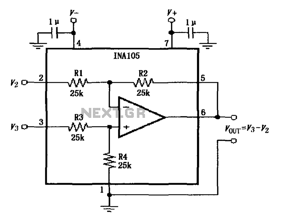
The circuit employs a 1 µF chip capacitor filter at the power supply terminal to stabilize the voltage supplied to the INA105 operational amplifier. This capacitor should be placed in close proximity to the chip's supply pins to minimize the effects of parasitic inductance and resistance, which can degrade the performance of the circuit.
The INA105 is a precision instrumentation amplifier designed for applications requiring high accuracy and low noise. The input pins 2 and 3 are used to receive the differential signal, which is crucial for accurate measurements. It is essential that the source resistance of the signal feeding into these pins is equal to the input resistor of the INA105 to achieve optimal common-mode rejection. The common-mode rejection ratio (CMRR) is a critical parameter that defines the amplifier's ability to reject common noise signals that may be present on both input lines.
In scenarios where there is a mismatch in the source resistance, the CMRR can suffer significantly, resulting in an approximate degradation of 80 dB. This decline can severely impact the performance of the circuit, making it crucial to match the source resistance to the input resistor accurately. In cases where the source mismatch is known, implementing a resistor in series with the input resistor can effectively counteract the mismatch and help maintain a high CMRR. This additional resistor should be chosen carefully to ensure it does not introduce excessive noise or offset errors into the system.
Overall, attention to detail in the layout and component selection will enhance the performance of the INA105, ensuring accurate signal amplification in precision applications. As shown, the power supply terminal to use 1 F chip capacitor filter, and should be as close to the chip supply pin placement. Signal produced by 2 feet and 3 feet input, signa l source resistance should be equal INA105 input resistor to ensure a high common-mode rejection ratio. If the signal source resistance 5 mismatch, the common mode rejection ratio to decline by about 80dB.
If you know the source mismatch in series with the input resistor serve to maintain a high common mode rejection ratio effect.
Related Circuits
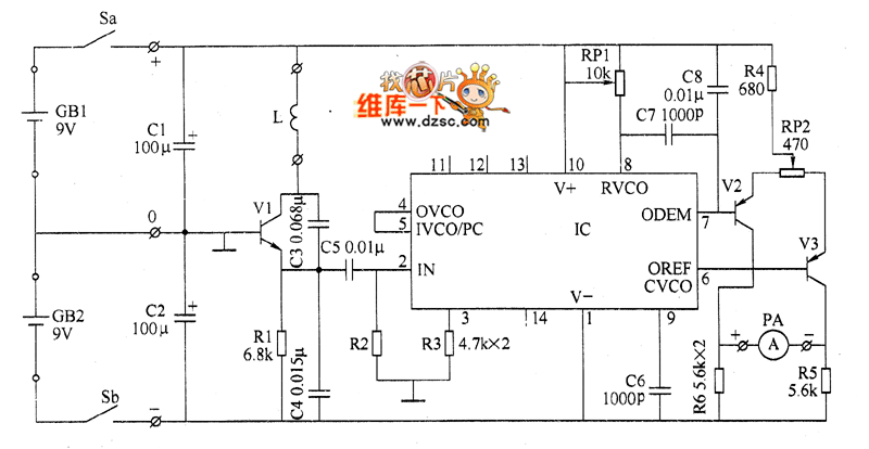
The metal detector circuit comprises several key components, including a power circuit, a sine wave oscillator, a PLL (phase-locked loop) circuit, and a hybrid amplifying circuit. The power circuit is made up of batteries GBI and GB2, filter capacitors...
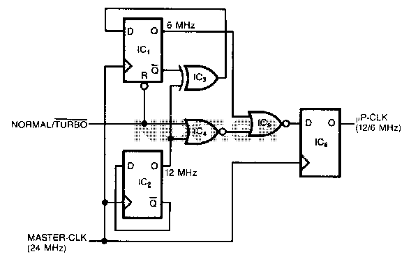
This circuit generates a dual-speed clock for personal computers. It synchronizes asynchronous switch inputs with the master clock to provide glitch-free transitions between clock speeds. The dual-speed clock allows certain programs to operate at a higher clock speed for...
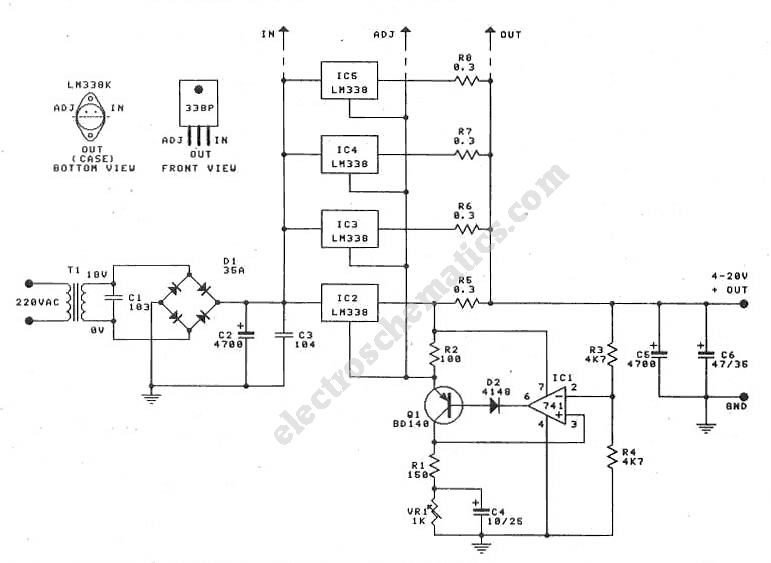
This is a regulated and adjustable power supply that can deliver up to 20A with an adjustable voltage range between 4V and 30V. It is straightforward to construct and utilizes the LM338 voltage regulator. The adjustable power supply circuit based...

This circuit has the advantage of transferring almost all the energy from the collapsing magnetic field of L2 to C2. In contrast, a typical Joule thief circuit allows some of this energy to return to the battery. This efficiency...
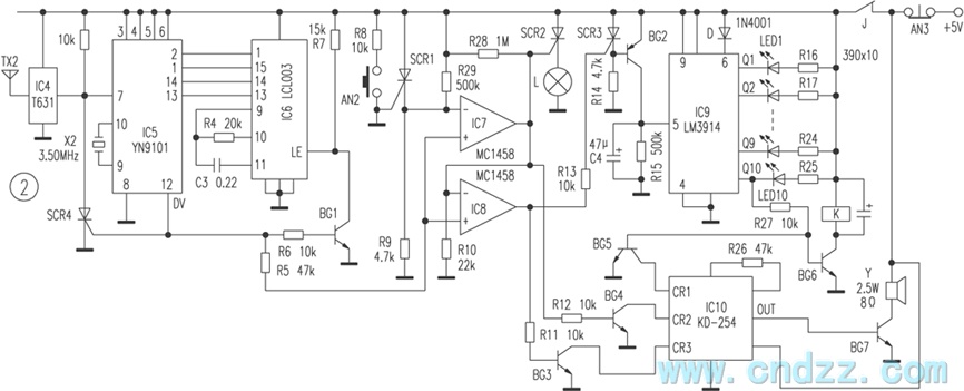
The wireless calling device consists of a calling unit and a host. These two components communicate using a DTMF encoder pulse. Each calling unit is assigned a unique code, although the circuits are identical. The calling unit is depicted...
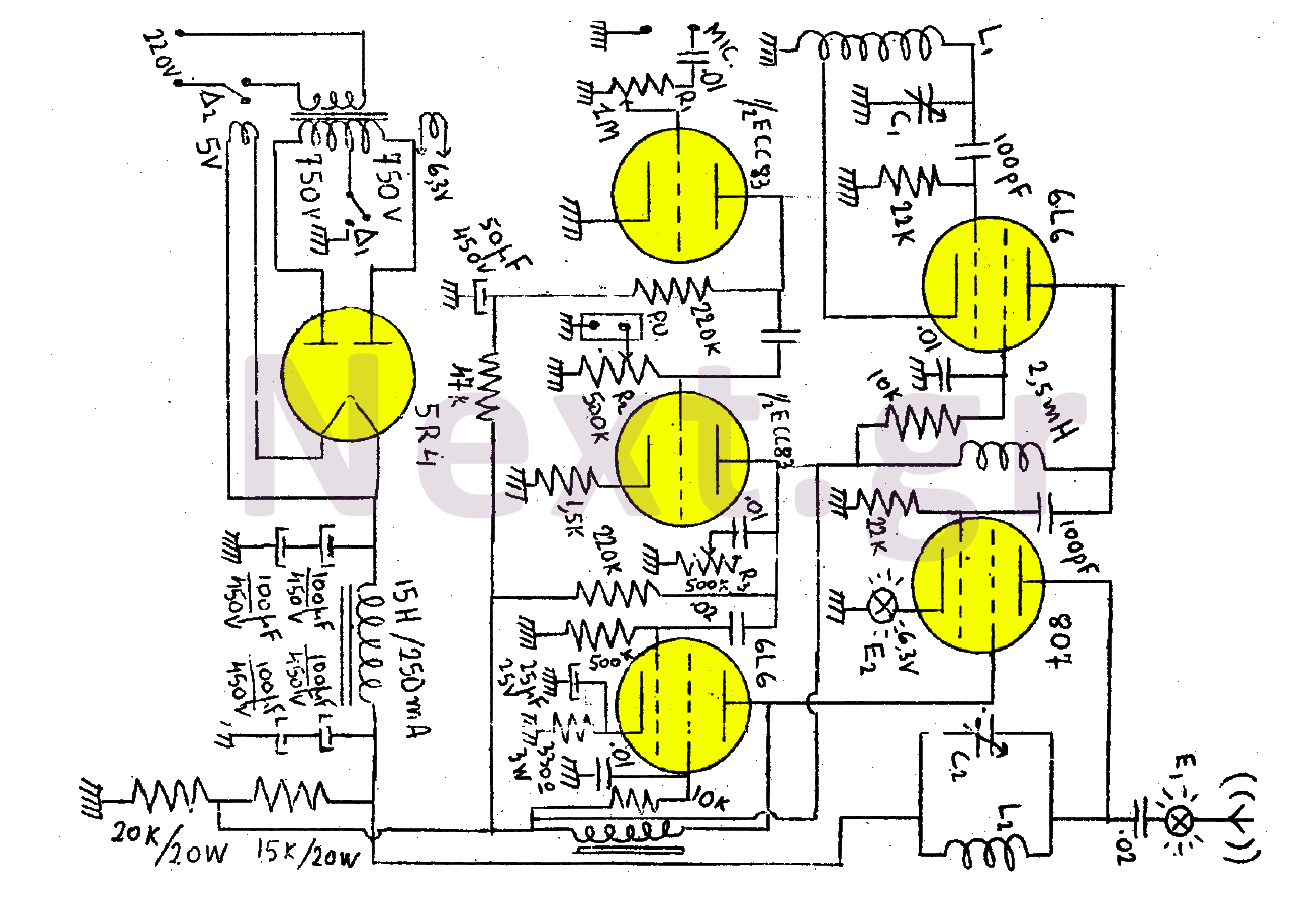
This transmitter consists of a total of five bulbs. The 6L6 tube functions as an oscillator, directing oscillations to the grid of the 807 tube, which serves as the final amplifier and the transmitter output lamp. The amplifier includes...