
Interpolating Scanner Circuit
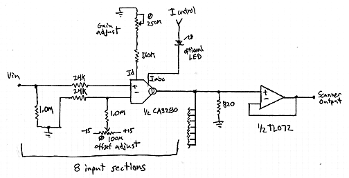
The interpolating scanner circuit operates by utilizing multiple current-controlled amplifiers (CCAs), where each CCA facilitates the processing of an individual signal input. The architecture allows for a seamless transition between inputs, enhancing audio mixing or signal routing applications. The design's reliance on a constant current source for the total drive current ensures stability in gain across all channels, which is crucial for maintaining audio fidelity during transitions.
The use of a differential amplifier topology in the drive circuit not only provides a robust control mechanism for the CCAs but also introduces versatility in handling various signal levels. By employing a buffer amplifier stage, the output can be adjusted to match the required impedance and voltage levels for downstream processing, thereby ensuring compatibility with other audio equipment.
The resistor network (R9 through R20) plays a pivotal role in creating the voltage steps necessary for controlling the CCAs. The diodes in the circuit are essential for selecting the appropriate voltage levels, ensuring that the most favorable signals are passed through to the outputs. This selection process contributes to the smooth fading effect that characterizes the interpolating scanner's performance.
Simulation results demonstrate the circuit's capability to produce predictable and controlled output currents in response to varying control voltages, confirming its effectiveness in practical applications. The ability to customize the interpolation curve further enhances the circuit's utility, making it suitable for a range of audio processing tasks, from simple panning to complex signal blending. Overall, the design leverages established principles in analog electronics while introducing innovations that improve performance and usability in real-world scenarios.This is an original design for an interpolating scanner, a circuit with a number of signal inputs, a control voltage input and a signal output. The output effectively selects between the inputs, fading from one to the next, as the control voltage rises.
A two-channel panner circuit might be considered a degenerate form of a scanner. The data sheet for the Precision Monolithics, Inc. SSM-2024 current-controlled amp IC shows a stereo panner, they call it an "Exponential Cross-Fade Controller", where two CCAs are controlled from a PNP differentialamp. The circuit is pretty straightforward and I`m sure similiar circuits have been used before. The circuit presented here is inspired by and similiar to JH`s scanner except that drive circuit is an unusual extrapolation of the differential amplifier topology used in the PMI panner.
This approach has some advantages: the total drive current (the sum of all the drive currents) is from a constant current source assuring that the sum of the individual gains is held constant Figure 1 below shows a block diagram of the Interpolating Scanner. There is a Current Controlled Amplifer (CCA) of traditional design for each signal input. Each CCA interfaces appropriately to the input signal, has a current source output, and a gain (transconductance) that is directly proportional to its control current input.
The CCA outputs are summed by shorting them directly together. A buffer amplifier stage provides the appropriate output level and impedance. The CCAs are transconductance amplifiers; the input is a voltage, the output is a current, the gain is linearly proportional to the control current, and in this case the control current is expected to be from 0. 0 to 2. 0 mA. More on this later. In the schematic above, the opamp provides a flexible interface to the outside world (you can add multiple inputs here as well as manual controls), scales the control voltage slightly, and supplies a low impedance source of the control voltage to the rest of the circuit.
The issue in extending a diff amp to more than two inputs is to not only gradually turn one transistor off and another on, but also turn that second one off and the next one on in the same manner. Resistors R9 through R14 provide 190mV voltage steps up from the control voltage and resistors R15 through R20 provide 190mV voltages steps up from ground.
The diodes select the higher of the two values. The X axis is the voltage tapped off of the opamp in volts and the Y axis is the various base voltages in volts. For clarity, the base voltages here are before the base diodes so offset everything down by one diode voltage drop to get the actual base voltages.
In the third plot we see the effect of the diodes, selecting the most positive of each of the voltage pairs. Again, for clarity this diagram shows voltages before the diode voltage drop. Note that the extreme outputs are not paired. Also note that the voltage between crossover points is two voltage steps. There is some control over the shape of the interpolation curve. The circuit presented above is optimized for a smooth and complete transition from one stage to the next, but by varying the control voltage swing and the difference between the voltage steps you can customize the curves.
Here are three plots from a SPICE simulation of the scanner drive circuit. All have the input control voltage on the X axis, 1 volt per division, and the individual output currents on the Y axis, 0. 5mA per division, with EIA colors representing output currents I1 through I8. 🔗 External reference
Related Circuits
The circuit utilizes relay control. The voice switch operates as follows: upon the first clap, the load (lights) is activated; upon the second clap, the load (lights) is deactivated. This system can be employed to control lighting in residential...
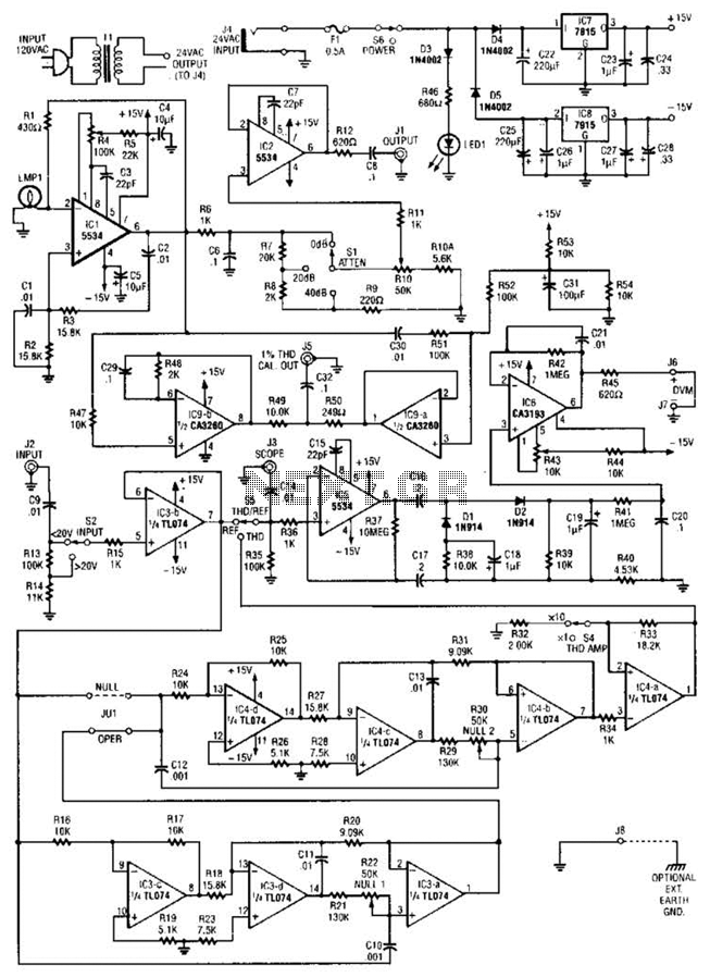
The circuit comprises a low-distortion, 1-kHz oscillator designed to measure Total Harmonic Distortion (THD) at a user-selected voltage level, suitable for voltage amplifiers or for testing amplifiers with power levels up to 600 W. It is capable of detecting...
The circuit presented is a 555 timer-based alarm system for vehicles, which primarily consists of a 555 timer and a quad 2-input NAND gate configuration. It is designed to produce a long beep sound when oil pressure is low...
Constantly changing light and sound analog controller circuit 05 The circuit described is an analog controller designed to modulate light and sound in a dynamic manner. This type of circuit typically employs a combination of resistors, capacitors, and operational amplifiers...
The tank circuit consisting of capacitor C2 and inductor L1 is utilized to tune the transmitter. The antenna is coupled to the transmitter through capacitor C3 and can be either a telescopic antenna or a length of hookup wire....
This is a simple freeze protector circuit diagram, also known as a timing circuit. It serves as a hobby project for beginners. This circuit can automatically operate any device after a fixed time once AC power supply is restored....
Warning: include(partials/cookie-banner.php): Failed to open stream: Permission denied in /var/www/html/nextgr/view-circuit.php on line 713
Warning: include(): Failed opening 'partials/cookie-banner.php' for inclusion (include_path='.:/usr/share/php') in /var/www/html/nextgr/view-circuit.php on line 713