
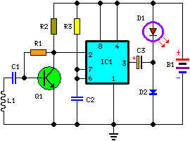
JAM (just a minute) circuit diagram
This circuit operates using several integrated circuits (ICs) and discrete components to achieve its functionality. The 74LS373 is a transparent latch that holds the state of the inputs when enabled. Resistors R1 through R8 serve to pull the input lines high when the reset switch is engaged. The 74LS147 functions as a priority encoder, determining which contestant's button was pressed first based on the input signals it receives. The 74LS30 NAND gate is used to create a logic condition that ensures only the first pressed switch is acknowledged, effectively "jamming" the output to prevent any subsequent inputs from changing the displayed number.
The buzzer is driven by a PNP transistor, which acts as a switch that is activated when the logic conditions are met. The reset mechanism is crucial for allowing multiple rounds of play, as it ensures that all outputs return to a known state before the next question is asked. The design focuses on simplicity and reliability, making it suitable for real-time quiz competitions where quick responses are essential. The inclusion of a manual reset switch adds to the control participants have over the game, ensuring a fair play environment. The circuit's design can be further enhanced or modified based on specific requirements or constraints of the quiz environment.This jam circuit can be used in quiz contests wherein any par- ticipant who presses his button (switch) before the other contestants, gets the first chance to answer a question. The circuit given here permits up to eight contestants with each one allotted a distinct number (1 to 8).
The display will show the number of the contestant pressing his b utton before the others. Simultaneously, a buzzer will also sound. Both, the display as well as the buzzer have to be reset manually using a common reset switch. Initially, when reset switch S9 is momentarily pressed and released, all outputs of 74LS373 (IC1) transparent latch go high since all the input data lines are returned to Vcc via resistors R1 through R8. All eight outputs of IC1 are connected to inputs of priority encoder 74LS147 (IC2) as well as 8-input NAND gate 74LS30 (IC3).
The output of IC3 thus becomes logic 0 which, after inversion by NAND gate N2, is applied to latch-enable pin 11 of IC1. With all input pins of IC2 being logic 1, its BCD output is 0000, which is applied to 7-segment decoder/driver 74LS47 (IC6) after inversion by hex inverter gates inside 74LS04 (IC5).
Thus, on reset the display shows 0. When any one of the push-to-on switches S1 through S8 is pressed, the corresponding output line of IC1 is latched at logic 0 level and the display indicates the number associated with the specific switch. At the same time, output pin 8 of IC3 becomes high, which causes outputs of both gates N1 and N2 to go to logic 0 state.
Logic 0 output of gate N2 inhibits IC1, and thus pressing of any other switch S1 through S8 has no effect. Thus, the contestant who presses his switch first, jams the display to show only his number. In the unlikely event of simultaneous pressing (within few nano-seconds difference) of more than one switch, the higher priority number (switch no.
) will be displayed. Simultaneously, the logic 0 output of gate N1 drives the buzzer via pnp transistor BC158 (T1). The buzzer as well the display can be reset (to show 0) by momentary pressing of reset switch S9 so that next round may start. Lab Note: The original circuit sent by the author has been modified as it did not jam the display, and a higher number switch (higher priority), even when pressed later, was able to change the displayed number.
Disclaimer: All the information present on this site are for personal use only. No commercial use is permitted without the prior permission from authors of this website. All content on this site is provided as is and without any guarantee on any kind, implied or otherwise. We cannot be held responsible for any errors, omissions, or damages arising out of use of information available on this web site.
The content in this site may contain COPYRIGHTED information and should not be reproduced in any way without prior permission from the authors. 🔗 External reference
Related Circuits
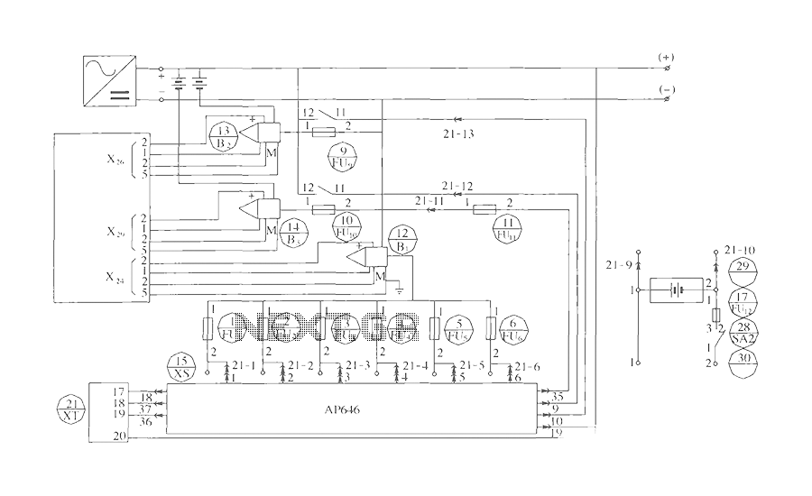
The components include B2 (13) and B3 (14) designated for the Hall current sensor; FU9 (9) and FU10 (10) serve as fuses; an AP646 alarm signal is connected to the fuse board; terminals X24, X26, and X29 function as...
The circuit operates by using a clock signal to drive four D-flip-flops in the control section, which store the on/off state of each current direction for the two stepper motor coils. The flip-flops create a finite state machine (FSM)...
The thermostat can be set, and it specifies the lower limit of the circuit diagram. The thermostat in the circuit is a critical component used to regulate temperature by controlling the heating or cooling system. It operates by comparing the...
If the TIP32C (Q2) transistor becomes excessively hot, consider replacing it with an IRF9640 MOSFET. It is advisable to experiment with different resistor values for R6 to determine the optimal resistance (a 390-ohm resistor is recommended). A trim potentiometer...

The PIC16F84A digital thermometer circuit is constructed primarily using a temperature sensor along with various discrete components. The PIC16F84A microcontroller serves as the core processing unit of the digital thermometer circuit. It is equipped with an 8-bit architecture and supports...
This circuit is designed to detect incoming calls on a cellular phone, even when the phone's ringer is turned off, by utilizing a flashing LED. The device should be positioned a few centimeters away from the cellular phone, allowing...