
Jfet sample and hold
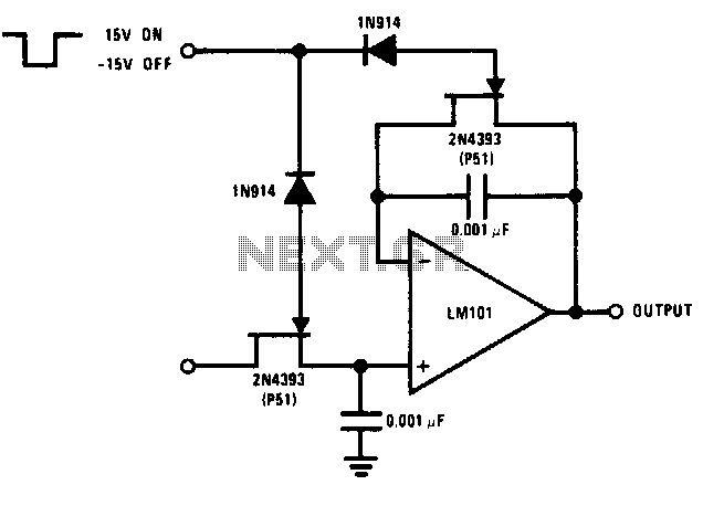
The circuit employs a sample and hold configuration utilizing Junction Field Effect Transistors (JFETs) to capture and maintain a voltage level for a specific duration. The simultaneous application of logic voltage to the JFETs ensures that the switching action occurs consistently, allowing for accurate sampling of the input signal.
To optimize performance, careful attention is given to matching the input impedance of the circuit with the feedback resistance and capacitance. This matching process is crucial as it helps to mitigate the errors introduced by the drain-source on-resistance (rdson) inherent in the JFETs. The rdson contributes to voltage drops that can lead to inaccuracies in the sampled signal, and by minimizing this effect, the integrity of the sampled data is preserved.
The schematic typically includes a pair of JFETs configured as a sample and hold circuit, where one JFET is responsible for sampling the input voltage while the other holds the sampled voltage steady. Additional components, such as operational amplifiers, may be integrated to buffer the output and provide necessary gain, further enhancing the circuit's performance. Capacitors are strategically placed to store the sampled voltage, while resistors are used to fine-tune the input impedance and feedback loop, ensuring optimal functionality and minimal signal distortion.
In summary, the design of the JFET-based sample and hold circuit emphasizes precision and accuracy through careful component selection and configuration, addressing potential errors to achieve reliable performance in various electronic applications.The logic voltage is applied simultaneously to the sample and hold JFETs By matching input impedance and feedback resistance and capacitance, errors due to rdston) of the JFETs are minimized. 🔗 External reference
Related Circuits
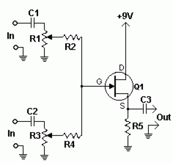
The 2N3819 is an n-channel JFET specifically designed for RF and mixer applications, offering very low noise, minimal distortion, and excellent high-frequency gain. Creating a PCB can be accomplished in a few straightforward steps. Begin by using PCB design...
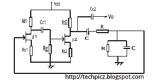
The Wien bridge oscillator utilizes a balanced Wien bridge as its feedback network. Two-stage common source amplifiers provide a 360-degree phase shift to the signal. The attenuation of the bridge is calculated to be 1/3 at the resonant frequency....
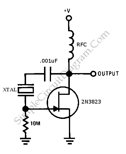
This is a simple JFET pierce crystal oscillator. A wide frequency range of crystals can be used with this circuit without requiring any modifications. The JFET pierce crystal oscillator is a versatile circuit that utilizes a Junction Field Effect Transistor...
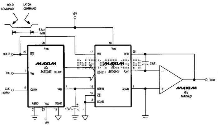
Driving a D/A converter using an A/D converter provides an overall analog-hold function. Although this function has limitations in output resolution, it offers zero voltage droop and infinite hold time. The A/D converter depicted (IC1) features a 12-bit compatible...
The LM4610 is a DC-controlled tone (bass/treble), volume, and balance circuit designed for stereo applications in car radios, televisions, and audio systems. It also incorporates National's 3D-Sound circuitry, which can be adjusted externally using a simple RC network. An...
The voice recorder's entry information can be stored for 100 years, repeated 100,000 times, with low power consumption. It requires a 5-6V DC power supply and has a recording current of 2 mA. The voice recorder circuit is designed to...