
Kapanadze 6

The described circuit involves the use of scope probes for measuring voltage and current in a system where isolation may not be present. In such cases, connecting the grounding leads of the probes to a common point (point A) while measuring at two different points (B and C) allows for the observation of current traces. It is crucial to note that the inversion of traces can be managed by adjusting the settings on the oscilloscope.
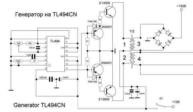
The schematic referenced includes the TL494, a popular PWM controller, which is commonly used in power supply applications. The internal transistors of the TL494 are essential for its operation, and the pin numbers indicated in blue circles aid in identifying their functions. This schematic serves as a guide for those constructing or analyzing similar circuits.
The discussion regarding MOSFETs highlights the importance of addressing issues related to internal parasitic diodes that can lead to undesired behavior in the circuit. The recommendation to utilize additional Schottky diodes or snubber circuits helps mitigate these effects by providing a path for reverse currents and reducing voltage spikes. The alternative suggestion of using transistors may lead to complications such as increased spiking, which should be carefully considered in the design process.
Incorporating 0.1 µF ceramic capacitors on the drain current paths, as illustrated in the schematic, further enhances the stability and performance of the circuit by filtering high-frequency noise and improving transient response. This design consideration is critical in ensuring the reliability and accuracy of the measurements obtained from the oscilloscope.If your scope probes are not isolated then it's still no problem because you can connect the grounding leads of your probes to point A and the tips of your probes to points B and C. Yes, the resulting current traces will be inverted, but only if you don't enable that inverting function in your scope's channel setup.
BTW: The schematic diagram below represents exactly what you have built, but it also shows the internal TL494 transistors (the numbers in blue circles are the TL494 pin numbers) and this schematic is just drawn in a different manner.
So this means any MOSFET with internal parasitic diodes are causing this, meaning use your suggested method of extra Shottky diodes/snubbers, or as an alternative; swap to transistors like in the diagram below? But then i probably will run in all sorts of other spiking problems, right? So i will go for the MOSFETs with Shottky diodes and my 17V snubber zeners. It is much better to put the 0.1Ω CSRs on drain current paths as illustrated on the attached diagram.
🔗 External reference
Related Circuits

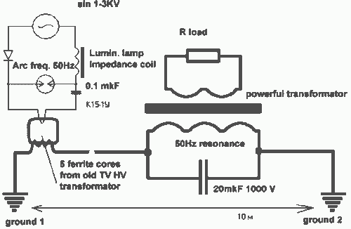
A thorough examination of the Kapanadze video reveals that the vertical coil is wound with copper tape, forming a capacitor that captures environmental particles with the assistance of high voltage. Experiments indicate that it charges easily with minimal power...
A Georgia Republic inventor, Tariel Kapanadze, claims to have invented a 5 kilowatt free energy generator. In a demonstration video, the device appears to produce copious amounts of energy from no visible source. More: The components apparently include a...
The 22-turn coil is positioned above the 84-turn coil. Connecting this coil significantly impacts performance. Testing with a 1 kW heater yielded better results; however, prolonged use may lead to failure. The heater's wire typically does not glow as...
The device features high-voltage (HV) insulation made of polystyrene. Incorporating ferrite may serve as a method to lower the frequency. However, using copper could lead to short circuits due to its interaction with radiant energy. It is noted that...
The Kapanadze device operates on the same principle as the oscillator-shuttle circuit discovered by Tesla over a century ago, and similarly aligns with concepts described by Bearden three decades ago regarding electrical free energy. This prior art may render...
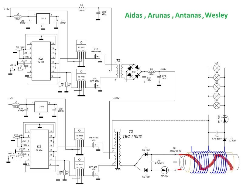
A circuit diagram has been found on a Russian website, freeenergylt.narod2.ru/Aidas. The diagram includes a pulse generator, which requires PCGU1000 equipment for the coils to function. There are discussions about the internal resonation design, involving a capacitor in parallel...