
Linear-triangle-wave-timer
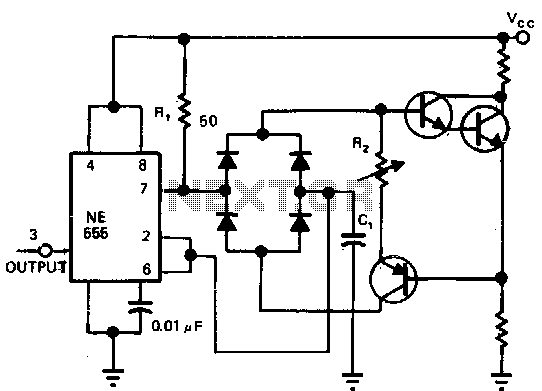
Utilizing a single current source for both the charge and discharge paths in this circuit guarantees that the rise and fall times at the capacitor terminal are identical. A Darlington pair is employed to ensure consistent biasing of the integrated circuit (IC) during both charge and discharge cycles. The period of the triangle wave is defined as T = 0.46VC1/R2. Additionally, Vcc must be a minimum of 8 V to preserve linearity. At the output of pin 3 of the IC timer, a square wave with a 50% duty cycle is generated, with frequency adjustable solely by R2.
The circuit design incorporates a current source that is pivotal for the charging and discharging processes of the capacitor (C1). This configuration results in uniform rise and fall times, which is critical for applications requiring precise timing and waveform characteristics. The Darlington pair configuration enhances the current gain, ensuring that the biasing of the IC remains stable throughout the operational phases of the circuit.
The triangle wave generated by the circuit is characterized by its period, which is mathematically defined as T = 0.46VC1/R2. Here, VC1 represents the voltage across the capacitor, and R2 is the resistance that influences the charging time. This relationship indicates that by adjusting R2, one can effectively control the frequency of the triangle wave, making it a versatile component in waveform generation.
Furthermore, the requirement for Vcc to be at least 8 V is crucial for maintaining the linear operation of the circuit. Lower voltages could lead to non-linear behavior, which would adversely affect the performance of the IC and the quality of the output waveform. The output at pin 3 of the timer IC produces a square wave with a 50% duty cycle, a desirable feature for many digital applications. The frequency of this output is solely dependent on the value of R2, allowing for straightforward tuning and adaptation to specific circuit needs. This design is particularly useful in applications such as signal generation, pulse width modulation, and timing circuits, where precise control over waveform characteristics is essential.Using one current source for tbe charge and discharge path in this circuit ensures identical rise and fall times at the capacitor terminal. A Darlington pair ensures identical biasing of the IC during the charge and discharge cycles. The period of the triangle wave is: T=0.46VC1/R2. Vcc must be at least 8 V to maintain linearity. At the output at pin 3 of the IC timer, a 50% duty-cycle square wave, frequency tunable by R2 alone, appears. 🔗 External reference