
Load test control circuit diagram
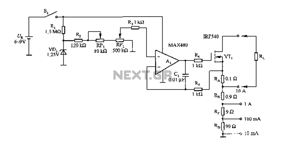
The FIG load test circuit is structured to provide precise control over load testing conditions. The integration of a power MOSFET (VT1) allows for efficient switching and management of high currents, while the sense resistors (RA and RD) are critical for monitoring the load current and ensuring accurate feedback to the control system. The use of a potentiometer (RP2) with a 10-turn configuration enables fine adjustments to the reference voltage, which is crucial for maintaining a stable output current during testing.
The operational amplifier (A1) plays a vital role in processing the feedback from the sense resistors, amplifying the error voltage to ensure that the load current remains within specified limits. The design includes provisions for stability enhancement through the use of capacitor C1, which mitigates any potential oscillations that may arise during operation.
Calibration procedures are essential for ensuring that the circuit operates within its intended specifications. By connecting the circuit to a known power source and adjusting the potentiometers, the user can establish a baseline for the output current. The ability to measure both 10A and 5A loads provides a comprehensive assessment of the circuit’s performance across its operational range.
In summary, the FIG load test circuit is a sophisticated electronic design that facilitates the testing of various electrical components under controlled conditions. Its focus on precision, stability, and adaptability makes it an invaluable tool in the field of electronics testing and validation.FIG load test is a control circuit. This external load circuit up to 10A, widely used in the drive test power, the power amplifier, LED solenoids and relays, and the carrying c apacity of the experiment. General resistive load different, it by a 1.2 50V voltage range adjustment load current to maintain a constant load test. Circuit power MOS-FET (VTl) and the sense resistor (RA a RD) load power consumption, battery used to isolate and solve the problem of grounding.
RP2 10-turn potentiometer, improve the accuracy and resolution. Wiper RP2 for Al provides a reference voltage through feedback to ensure prosperous wiper voltage present on R5, forcing the required load current through the VT1. Al bias current (up to 3nA) via an RD series resistor RA circulation, the current times and four resistors (100 obtained 30OnV error voltage.
This compared with the error voltage to provide the noninverting input of A1 by the voltage RP2 is small, negligible .Cl for enhancing stability, RA RD series resistor can be a 4 range of output current. During calibration, access the battery and the circuit, and then access 5V/l0A power as experimental load RL.
In RP2 for the next full-scale, adjusting RPl and read the exact 10 OOA current with ammeter. In order to check the linearity of the circuit, to accurately adjust the RP2, and reads 5, OOA current with ammeter. RB RD adjust a resistance calibration to the rest of the current range.
Related Circuits
This is a square wave oscillator (digital, similar to 8-bit music). It is based on the LM386 amplifier integrated circuit, which is also the foundation for the mini guitar amplifier. The design includes a simple power switch connected to...
There are monitors that feature only three BNC inputs and utilize composite synchronization (sync on green). This circuit has been specifically designed for such monitors. The design maintains simplicity while delivering reasonable performance. The operational principle is straightforward. The...
A circuit involving oscillations is composed of a Houle Wang oscillator that utilizes a transistor configuration with components labeled Ti, n, and n, along with a composition of Q constants for the cycle. The waveform can be modified by...
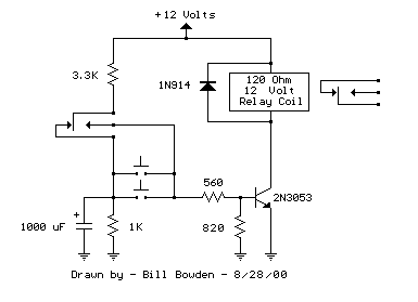
The circuit requires a double pole, double throw relay in conjunction with a single transistor to allow toggling the relay with a momentary push button. One set of relay contacts is used to control the load, while the other...
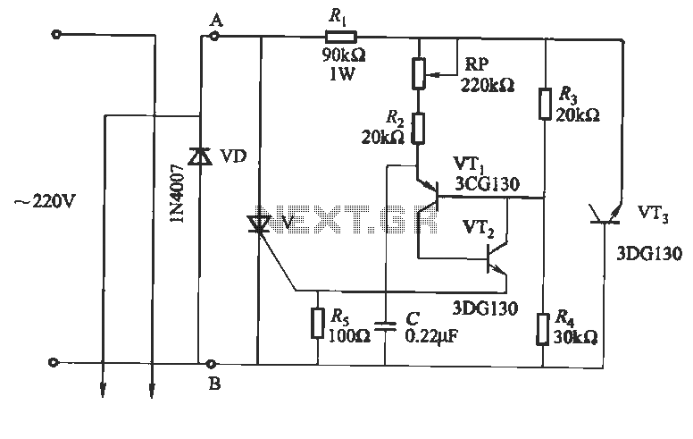
This circuit utilizes an "and other potential triggers" circuit. The term equipotential trigger refers to a crystal bidirectional thyristor trigger, which can be activated by either a positive or negative trigger. In this setup, the control electrode G and...
The shutter speed tester integrates a frequency counter, a crystal oscillator, and a photo-transistor-operated gate generator. The oscillator generates pulses that are counted while the shutter remains open. Additionally, the reset occurs automatically at the moment the shutter opens. The...