
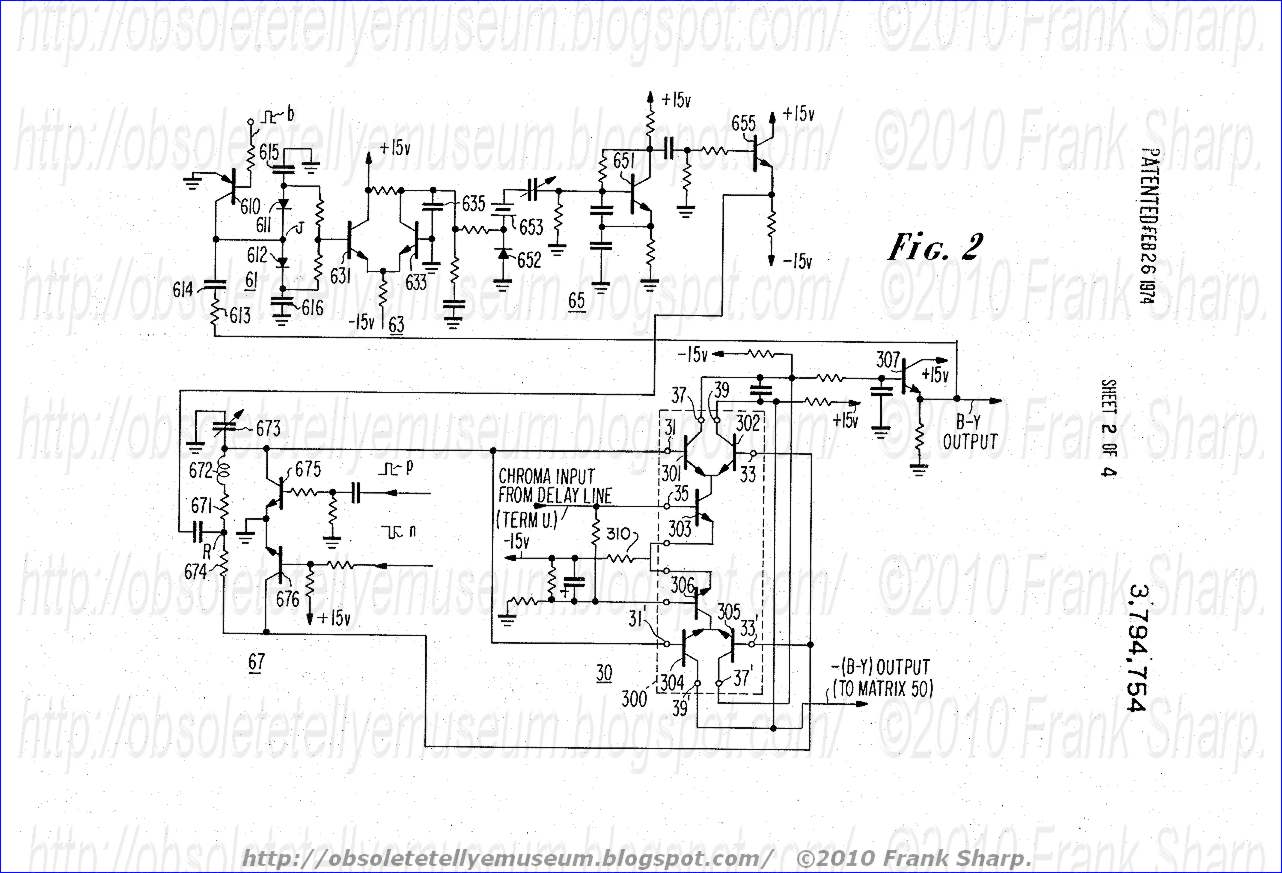
loewe f875 sensotronic chassis f800 11

The LOEWE F875 SENSOTRONIC CHASSIS 543/490 is based on the F800 LOEWE chassis series and functions similarly to a color television chassis, featuring an EHT output with a tripler and horizontal output utilizing thyristor technology. The LOEWE-OPTA start-delay overload protection arrangement for a thyristor sweep circuit includes an input switching thyristor of the deflection circuit that is selectively activated at a sweep rate by a transistorized driver stage. A separate protective thyristor is situated in a DC power source that provides operating bias to both the driver stage and the switching thyristor through a supply capacitor. Initially, the supply capacitor is partially charged via a high-ohmic shunt resistor, which activates the protective thyristor, with its control electrode connected to the output of the switching thyristor. A portion of the voltage across the partially charged supply capacitor is routed through a voltage divider and a Zener diode to the base of a threshold-operated transistor that typically blocks the driver stage. When the supply capacitor reaches a predetermined minimum charge necessary for the protective thyristor to turn on, the threshold-operated transistor is triggered, allowing the driver stage to operate the switching thyristor at the sweep rate. The activation of the protective thyristor facilitates the rapid charging of the supply capacitor to its normal operating voltage, thereby providing full overload protection for the deflection circuit.
In a communications receiver, the system includes a first input switching thyristor of a deflection circuit pulsed at a sweep rate by a driver stage when excited, a supply capacitor chargeable through a second protective thyristor bypassed by a high-impedance shunt, providing operating bias to both the driver stage and the switching thyristor. The output of the switching thyristor is connected to the control electrode of the protective thyristor. The enhancements to this system consist of a gating mechanism that includes a first transistor with its collector-emitter path connected in series with the driver stage. The coupling mechanism involves a voltage divider connected across the supply capacitor, with the output of the voltage divider applied to the base of the first transistor, utilizing a Zener diode for voltage regulation. The driver stage may include a second transistor, with the first and second transistors operating with opposite conductivity types.
A standard horizontal sweep circuit for a communications receiver features an input switching thyristor that triggers the flyback phase at the deflection transformer. The control electrode of the switching thyristor receives pulses at a sweep rate from a transistorized driver stage, whose base is linked to a horizontal oscillator's output. A common DC power source, connected to the AC mains, supplies operating bias to the switching thyristor and the driver stage via an output supply capacitor. To ensure overload protection for the deflection circuit, a second protective thyristor is arranged in shunt with a high-ohmic bypass resistor in the DC power path between the main rectifier and the supply capacitor. The output voltage of the switching thyristor, which is determined by the operating bias magnitude, is fed back in an integrated form to the control electrode of the protective thyristor, maintaining it in a conductive state as necessary. In the event of an overload in the deflection circuit, the output voltage of the switching thyristor decreases to a level insufficient to trigger the protective thyristor, thus safeguarding the overall system.The LOEWE F875 SENSOTRONIC CHASSIS 543/490 is realized with the F800 LOEWE Chassis serie and in the Line / Horizontal deflection output like a COLOR TELEVISION CHASSIS with EHT output with Tripler and Horizontal output with thyristor tech. LOEWE-OPTA Start-delay overload protection arrangement for a thyristor sweep circuit:An input switching thyri
stor of a deflection circuit is selectively excited at a sweep rate by a transistorized driver stage. A separate protective thyristor is disposed in a DC power source that supplies operating bias to the driver stage and to the switching thyristor via a supply capacitor.
Initially, the supply capacitor is partially charged through a high-ohmic shunt resistor that budges the protective thyristor, whose control electrode is coupled to the output of the switching thyristor. A portion of the resulting voltage across the partially charged supply capacitor is applied via a voltage divider and a Zener diode to the base of a threshold-operated transistor that normally blocks the driver stage.
When the supply capacitor has charged to a predetermined minimum value necessary to assume turn-on of the protective thyristor, the threshold-operated transistor is triggered to permit the driver stage to operate the switching thyristor at the sweep rate. The resulting turn-on of the protective thyristor permits the rapid completion of charge of the supply capacitor to its normal operating voltage, and thereafter provides full overload protection for the deflection circuit.
1. In a communications receiver wherein (a) a first input switching thyristor of a deflection circuit in the receiver is pulsed at a sweep rate by a driver stage when the latter is excited, (b) a supply capacitor is chargeable through a second protective thyristor by-passed by a high-impedance shunt to provide operating bias to both the driver stage and the switching thyristor, and, (c) the output of the switching thyristor is coupled to the control electrode of the protective thyristor, the improvement which comprises: 2. The improvement as defined in claim 1, in which the gating means comprises a first transistor having its collector emitter path connected in series with the driver stage, and in which the coupling means comprises, in combination, a voltage divider having its input terminals connected across the supply capacitor, and means for applying the output of the voltage divider to the base of the first transistor.
3. The improvement as defined in claim 2, in which the applying means comprises a Zener diode. 4. The improvement as defined in claim 2, in which the driver comprises a second transistor, and in which the first and second transistors are of opposite conductivity type. One conventional horizontal sweep circuit for a communications receiver has an input switching thyristor which is excitable to trigger the flyback phase at the deflection transformer.
For this purpose, the control electrode of the switching thyristor is supplied with pulses at a sweep rate via a transistorized driver stage, whose base is coupled to the output of a horizontal oscillator. A common DC power source coupled to AC mains provides operating bias to the switching thyristor and to the driver stage via an output supply capacitor.
In order to provide overload protection of the deflection circuit it has been proposed to arrange a second protective thyristor in shunt with a high-ohmic bypass resistor in the DC power sound between the main rectifier and the supply capacitor. The voltage at the output of the switching thyristor (determined by the magnitude of the operating bias) is fed back in integrated form to the control electrode of the protective thyristor to maintain the latter in a conductive stage as required.
In the presence of an overload in the deflection circuit, the output voltage of the switching thyristor drops to a value insufficient to trigger the protective thyristor 🔗 External reference
Related Circuits
A multiple automatic brightness control system for a television receiver includes a first automatic brightness limiter (ABL) circuit that responds solely to relatively long-duration changes in brightness-producing current and a second ABL circuit that reacts to shorter-duration changes in...