
Long delay timer using put
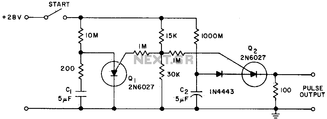
The Programmable Unijunction Transistor (PUT) is a semiconductor device that is widely utilized in various timing and oscillator applications due to its unique characteristics. In circuits where the PUT is employed, it functions by generating a timing pulse or oscillation based on external components such as resistors and capacitors. The timing element aspect of the PUT allows for precise control over the duration and frequency of the output signal.
In this specific application, capacitor C2 plays a critical role in the performance of the circuit. The requirement for a low leakage film capacitor is essential because any leakage current can significantly affect the timing accuracy and stability of the oscillator. A low leakage capacitor ensures that the charge stored within the capacitor is maintained effectively, allowing for more reliable operation of the timing circuit.
The selection of components in conjunction with the PUT is crucial for achieving the desired performance. Resistors connected to the PUT will determine the timing intervals, while the value and type of capacitor will influence the frequency of oscillation. Additionally, the circuit layout should be designed to minimize parasitic capacitance and inductance, which can introduce unwanted variations in timing and frequency response.
Overall, the integration of the PUT as a timing element and sampling oscillator, along with the careful selection of a low leakage film capacitor for C2, forms the foundation of a stable and precise electronic timing circuit.The PUT is used as both a timing element and sampling oscillator A low leakage film capacitor is required for C2 due to the low current supplied to it. 🔗 External reference
Related Circuits
The 50W inverter circuit is built using the power MOSFET FQB45N03 and the IC TL494. This inverter converts a 12-14V DC input from a car battery into a 220V AC output with a 50Hz sine wave frequency. The main...
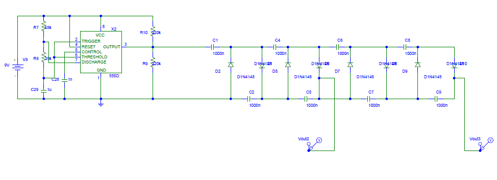
This circuit operates as a 9V DC power source supplying a 555 timer to generate a square wave. The output is then processed through a Half-Wave Series Multiplier (Villard Cascade) to achieve a high voltage DC output. The goal...
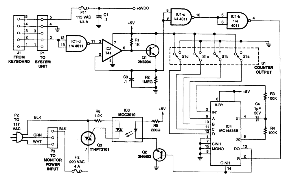
The circuit monitors PC keyboard activity through a five-pin DIN connector J1. When a key is pressed, the keyboard transmits a series of negative-going pulses on pin 2. In conjunction with Q1 and C3, the operational amplifier operates as...

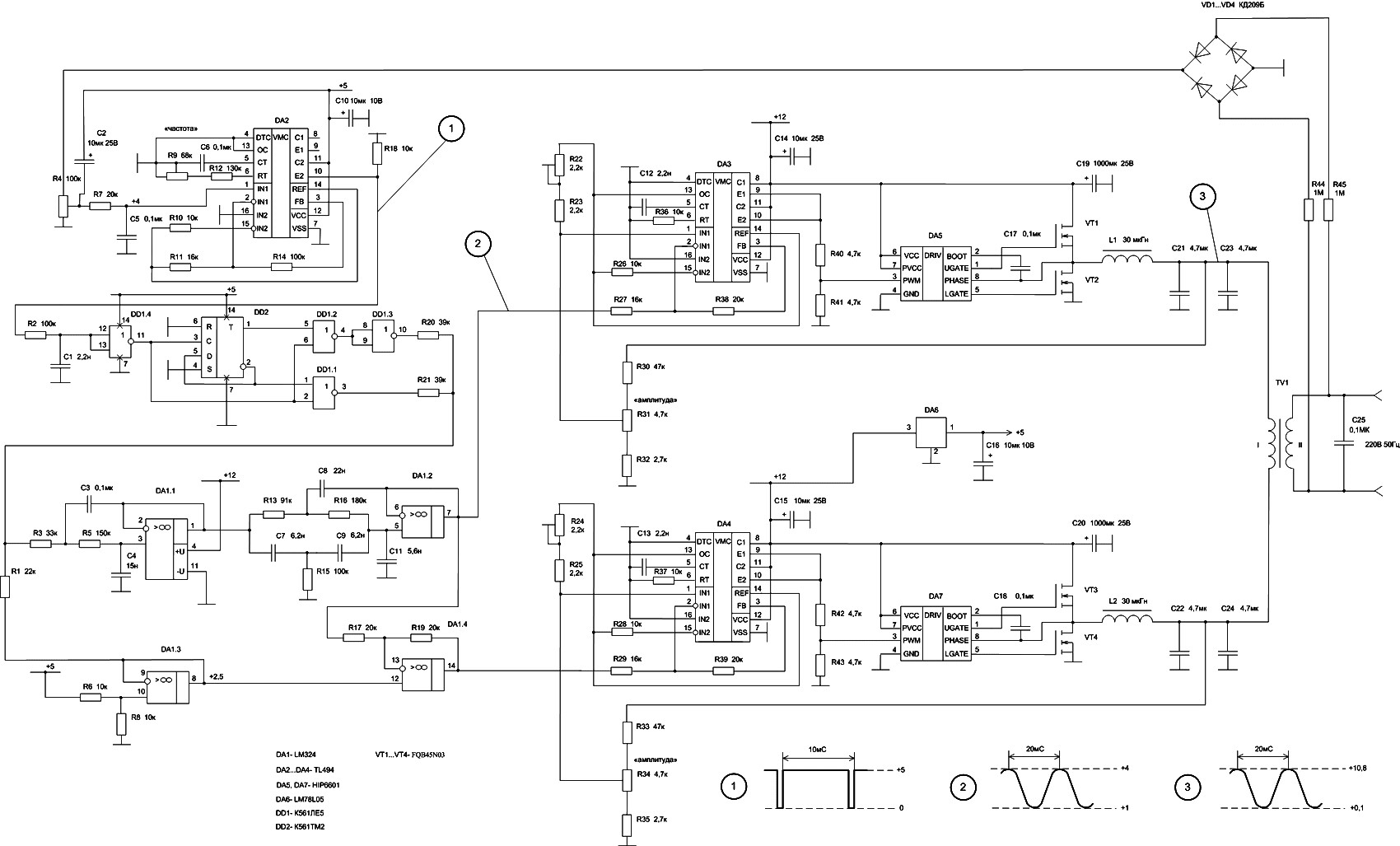
In DA3, DA5, VT1, and VT2, the first channel of the VLF Class D amplifier is assembled. The second channel is constructed using DA4, DA7, VT3, and VT4. Antiphase sine waves in the VLF range are formed at the...
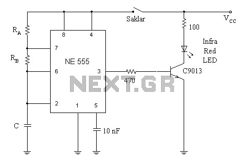
A simple circuit diagram illustrates a schematic for a remote control system, which consists of two components: a transmitter and a receiver. The transmitter circuit is controlled by the NE555 integrated circuit (IC). This system operates by detecting the...
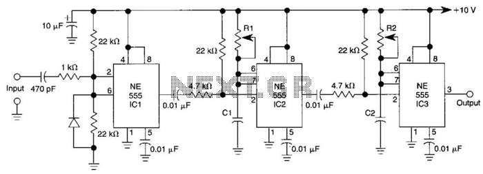
Three 555 IC timers are utilized in this circuit to create a simple delayed-pulse generator. IC1 functions as a waveform shaper to generate a rectangular waveform. IC2 generates a delaying pulse that triggers IC3 on the trailing edge of...