
Low-cost-fsk-generator
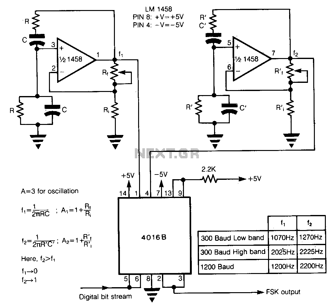
In Frequency Shift Keying (FSK), two distinct frequencies are utilized to represent the binary digits 0 and 1. The core of the circuit comprises two Wien-bridge oscillators constructed with a dual operational amplifier LM1458, each generating one of the two frequencies. These frequencies are activated in correspondence with the digital data through the use of two switches in the SCL 4016. The control lines of these switches are logically inverted relative to one another by employing one of the switches in the SCL 4016 as an inverter, ensuring that only one oscillator output is enabled at any given time. The digital bit stream is used to control the analog switches as illustrated. With a switching frequency limit of 40 MHz for the SCL 4016, high data rates can be effectively managed. This approach is particularly useful when expensive FSK generator chips are not readily available; additionally, the components utilized in this circuit are easily obtainable and cost-effective.
The circuit design for this FSK implementation effectively leverages the properties of Wien-bridge oscillators, which are known for their stability and low distortion in generating sine waves. The dual LM1458 operational amplifier is configured to create two separate oscillators, each tuned to a specific frequency that corresponds to the binary states. The Wien-bridge configuration typically includes resistors and capacitors that set the oscillation frequency, thus allowing for precise control over the generated sine waves.
The SCL 4016, a quad bilateral switch, plays a crucial role in this circuit by enabling the selection of the appropriate oscillator output based on the digital input. The logical inversion of the control lines ensures that when one oscillator is active, the other remains inactive, preventing signal interference and ensuring a clean output. This switching mechanism is vital for effectively encoding the digital data stream into an analog format suitable for transmission.
The high-frequency capability of the SCL 4016 allows for the accommodation of rapid data rates, making this circuit suitable for various applications where bandwidth is a consideration. The choice of readily available components not only reduces costs but also simplifies the assembly and maintenance of the circuit. Overall, this FSK circuit design exemplifies an efficient and economical solution for digital communication applications, particularly in scenarios where specialized FSK generator chips are not feasible.In FSK, two discrete frequencies are used to represent the binary digits 0 and 1. The heart of the circuit consists of two Wien-bridge oscillators built using a dual op amp LM 1458, for the two frequencies. The two frequencies are enabled corresponding to digital data using two switches in SCL 4016. The control lines of these switches are logically inverted with respect to each other using one of the switches in SCL 4016 as an inverter, so as to enable only one oscillator output at a time.
The digital bit stream is used to controLthe analog switches as shown. Since the switching frequency limit of SCL 4016 is 40 MHz, highdata rates can be easily accommodated. This method comes in handy when expensive FSK generator chips are not readily available; also, the components used in this circuit are easily available off the shelf and are quite cheap.
🔗 External reference