Low-cost-voltage-to-frequency-converter

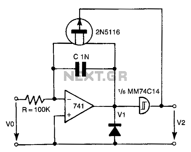
The 741 operational amplifier integrator signal is input into the Schmitt trigger of an inverter. When the signal reaches the positive-going threshold voltage, the inverter's output switches to zero. This output directly controls the FET switch. With a gate voltage of zero, the FET channel enters a low-resistance state, allowing the capacitor to discharge. The discharge current is determined by the on-resistance of the FET. When the capacitor C1 discharges to the negative-going threshold voltage level of the inverter, the inverter's output switches to ±12 V. This transition causes the FET channel to turn off, shifting the discharging process back into a charging phase. With the specified components, an output frequency of approximately 10 kHz with 0.1% linearity can be achieved.
The described circuit employs a 741 operational amplifier configured as an integrator, which generates a ramp signal based on the input voltage. This ramp signal is fed into a Schmitt trigger, which provides hysteresis and ensures clean switching behavior. The Schmitt trigger's thresholds define the points at which the inverter output toggles, allowing for precise control of the output signal.
When the ramp signal from the integrator exceeds the positive threshold voltage, the inverter output transitions to zero volts. This condition effectively turns on the FET switch, creating a low-resistance path that allows the connected capacitor, C1, to discharge. The rate of discharge is influenced by the on-resistance of the FET, which is a critical parameter for determining the discharge current.
As the voltage across C1 decreases and reaches the negative-going threshold of the inverter, the inverter output switches to ±12 V. This transition deactivates the FET switch, halting the discharge process and initiating a charging phase for the capacitor. The switching behavior of the inverter and the associated FET allows for the generation of a square wave signal, with the frequency of oscillation primarily dictated by the values of C1 and the resistive components in the circuit.
The design can achieve an output frequency of around 10 kHz while maintaining linearity of 0.1%. This level of performance is suitable for various applications, including waveform generation and signal processing tasks in electronic systems. Proper selection of components and careful consideration of the circuit layout will contribute to the overall effectiveness and reliability of the circuit.The 741 op amp integrator signal is fed into the Schmitt trigger input of an inverter. When the signal reaches the magnitude of the positive-going threshold voltage, the output of the inverter is switched to zero. The inverter output controls the FET switch directly. For a gate voltage of zero, the FET channel turns on to low resistance and the <:apacitor is discharged. The discharge current depends on the on resistance of the FET. When the capacitor C1 is discharged to the negative-going threshold voltage level of the inverter, the inverter output is switched to ±12 V. This switch causes the FET channel to be switched off, and the discharging process is switched into a charging process again.
Using the components shown, an output frequency of about 10kHz with 0.1 % linearity can be obtained.