
Low-distortion-video-buffer
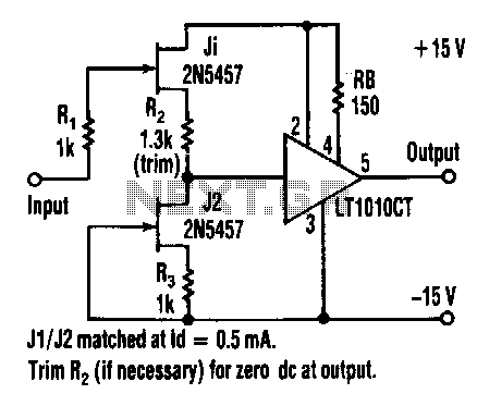
This buffer amplifier's overall harmonic distortion is low at 0.01% or less at a 3-V RMS output into a 500-ohm load without overall feedback. The LT1010CT features a slew rate of 100 V/µs, a video bandwidth of 20 MHz, and an output current capability of 100 mA. A pair of JFETs, J1 and J2, are preselected for a nominal match at the bias level of the linearized source-follower input stage, approximately 0.5 mA. The source bias resistor, R2, of J1 is somewhat larger than R3 to drop a larger voltage and cancel the offset of the LT1010CT. J1 and J2 provide an untrimmed DC offset of ±50 mV or less.
Swapping J1 and J2 or adjusting the value of R2 can yield a finer match. The circuit's overall harmonic distortion remains low at 0.01% or less at a 3-V RMS output into a 500-ohm load without overall feedback. The circuit's response to a ±5 V, 10 kHz square-wave input, band-limited to 1 µs, shows no overshoot. If necessary, lowering the bias resistor R8 can accommodate steeper input signal slopes and drive lower impedance loads with high linearity. The primary trade-off for achieving these objectives is increased power dissipation, and a secondary trade-off involves the need for retrimming the source-bias resistor, R2.
This buffer amplifier circuit utilizes the LT1010CT operational amplifier to achieve high performance in terms of linearity and low distortion. The choice of JFETs, J1 and J2, is critical for maintaining the desired input characteristics, ensuring that the input stage operates efficiently within the specified bias current. The design emphasizes the importance of matching the JFETs to minimize offset voltage, which can be further refined by adjusting the source bias resistor R2.
The circuit's harmonic distortion specification of 0.01% or less indicates excellent fidelity for audio and video applications, making it suitable for high-quality signal processing. The slew rate of 100 V/µs allows the amplifier to respond rapidly to changes in input signal, which is essential in applications involving fast transients, such as video signals.
The ability to handle a 3-V RMS output into a 500-ohm load without feedback showcases the amplifier's robustness and versatility. The design considerations for accommodating various input signal profiles, including the adjustment of R8 for steeper slopes, highlight the adaptability of the circuit to different operational requirements.
In summary, this buffer amplifier circuit is engineered for high performance, low distortion, and adaptability, making it an excellent choice for applications requiring precise signal amplification with minimal degradation. The trade-offs involved in power dissipation and the need for potential retrimming of bias resistors are essential considerations for designers aiming to optimize the amplifier's performance in practical applications.This buffer amplifier"s overall harmonic dis tortion is a low 0.01 % or less at 3-V rms output into a 500-fl load with no overall feedback. The LT1010CT offers a 100 V/p.s slew rate, a 20 MHz video bandwidth, and 100 mA of output. A pair of JFETs, ]1 and J2 are preselected for a nominal match at the bias level of the linearized source-follower input stage, at about 0.5 mA.
The source: bias resistor, R2, of ]1 is somewhat larger thao R3 so that it cao drop a larger voltage aod cancel the LT1010CT"s offset. J1 andJ2 provide ao untrimmed de offset of ±50 mV or less. Swapping ]1 and J2 or trimming the R2 value cao give a finer match. The circuit"s overall harmonic distortion is low: 0.01 % or less at 3-V rms output into a 500-fl load with no overall feedback. The circuit"s response to a ± 5 V, 10kHz square-wave input, band-limited to 1 p.s, has no overshoot.
lf needed, setting bias resistor R8 lower cao accommodate even steeper input-signal slopes and drive lower impedance loads with high linearity. The main trade-off for both objectives is more power dissipation. A secondary trade-off is the need for retrimming the source-bias resistor, R2. 🔗 External reference