
max2338 hp at the sound amplifier
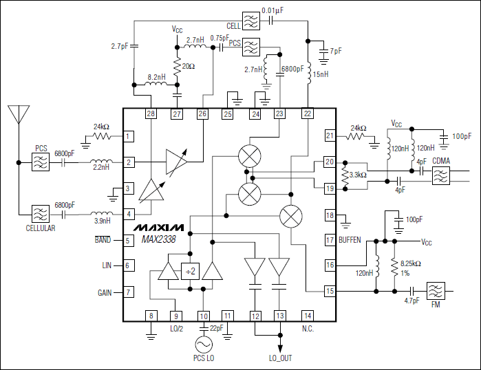
The MAX2338 RF front-end integrated circuit serves as a versatile solution for dual-band cellular applications, providing significant enhancements in performance and efficiency. The elimination of the cellular VCO module through the on-chip low-power LO divider not only simplifies the design but also contributes to the overall reduction in power consumption, which is critical for battery-operated devices such as mobile phones.
The low-noise amplifier (LNA) integrated within the MAX2338 is crucial for enhancing signal quality by amplifying weak incoming signals while minimizing noise. The adjustable high-input third-order intercept point (IIP3) feature allows for fine-tuning to optimize performance in environments with strong interfering signals, thereby improving the linearity of the system. The option for a low-gain LNA specifically tailored for cellular band operations is a strategic design choice, as it enables higher cascaded IIP3 values while maintaining lower power consumption, aligning with the current trends in mobile technology towards energy efficiency.
The mixers designed for CDMA applications prioritize high linearity and low noise, which are essential for maintaining signal integrity in complex communication environments. The differential IF outputs further enhance noise performance and signal fidelity. In contrast, the FM mixer is optimized for lower current consumption, making it suitable for applications where power efficiency is paramount.
The incorporation of an on-chip LO frequency divider within the MAX2338 facilitates the use of a single voltage-controlled oscillator (VCO) for both frequency bands, streamlining the design and reducing component count. This integration not only saves space but also contributes to the overall reliability of the system by minimizing the number of external components.
The MAX2338 is packaged in an ultra-small 28-pin leadless QFN format, which is advantageous for modern mobile phone designs that require compact and efficient layouts. The leadless design enhances thermal performance and simplifies PCB assembly processes, making the MAX2338 an ideal choice for manufacturers aiming to optimize both performance and size in their cellular devices.The MAX2338 receiver RF front-end IC is designed for dual-band CDMA cellular phones and can also be used in dual-band TDMA, GSM, or EDGE cellular phones. Thanks to the MAX2338 ²s on-chip low-power LO divider, the cellular VCO module can be eliminated. The includes a low-noise amplifier (LNA) with an adjustable high-input third-order intercept poi nt (IIP3) to minimize inter modulation and cross-modulation in the presence of large interfering signals. For cellular band operation, a low-gain LNA is available for higher cascaded IIP3 at lower current. The CDMA mixers are designed for high linearity, low noise, and differential IF outputs. The FM mixer is designed for lower current and single-ended output. The MAX2338 triple-mode LNA/mixer includes an on-chip LO frequency divider to allow the use of a single VCO for both bands.
This device is available in an ultra-small 28-pin leadless QFN package. 🔗 External reference
Related Circuits
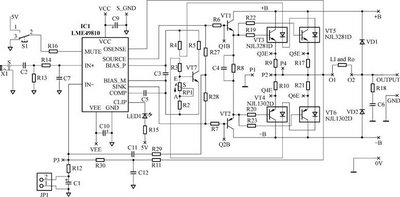
The following circuit illustrates the LME49810 integrated circuit used in a power amplifier circuit diagram. Features include improved drive capability for 4-ohm speaker impedance. The LME49810 is a high-performance audio power amplifier IC designed to deliver high output power with...
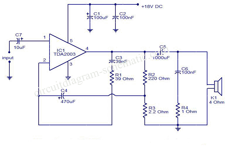
This is a circuit diagram of an audio amplifier circuit featuring a 10W power amplifier using the TDA2003 integrated circuit from SGS Thomson. The IC is capable of delivering 10W into a 4-ohm load at a supply voltage of...
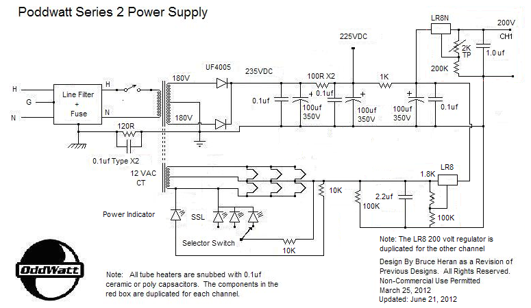
This project is related to previous tube amplifier designs, particularly the first Push-Pull EL84 (6BQ5) Oddwatt project from nearly two years ago. Both projects utilize EL84 / 6BQ5 tubes; however, while the earlier version employed an ECC802S driver, this...
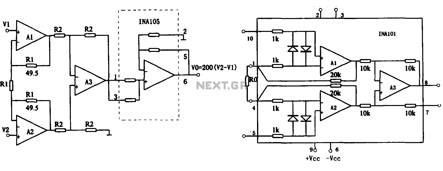
This document describes the extended common mode input voltage range of an instrument amplifier circuit. The circuit consists of three precision instrument amplifiers, A1, A2, and A3, which can be INA101 or INA102 models. The figure illustrates that A1,...
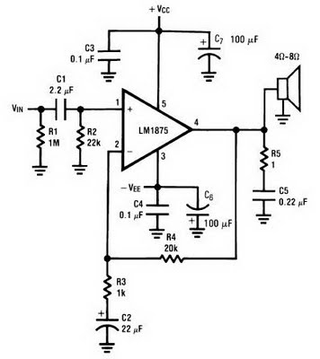
The amplifier circuit can be constructed using the LM1875 power amplifier IC. The LM1875 is a single-chip power amplifier from National Semiconductor. This 20-watt audio amplifier is characterized by low power consumption while delivering high-quality sound suitable for use...
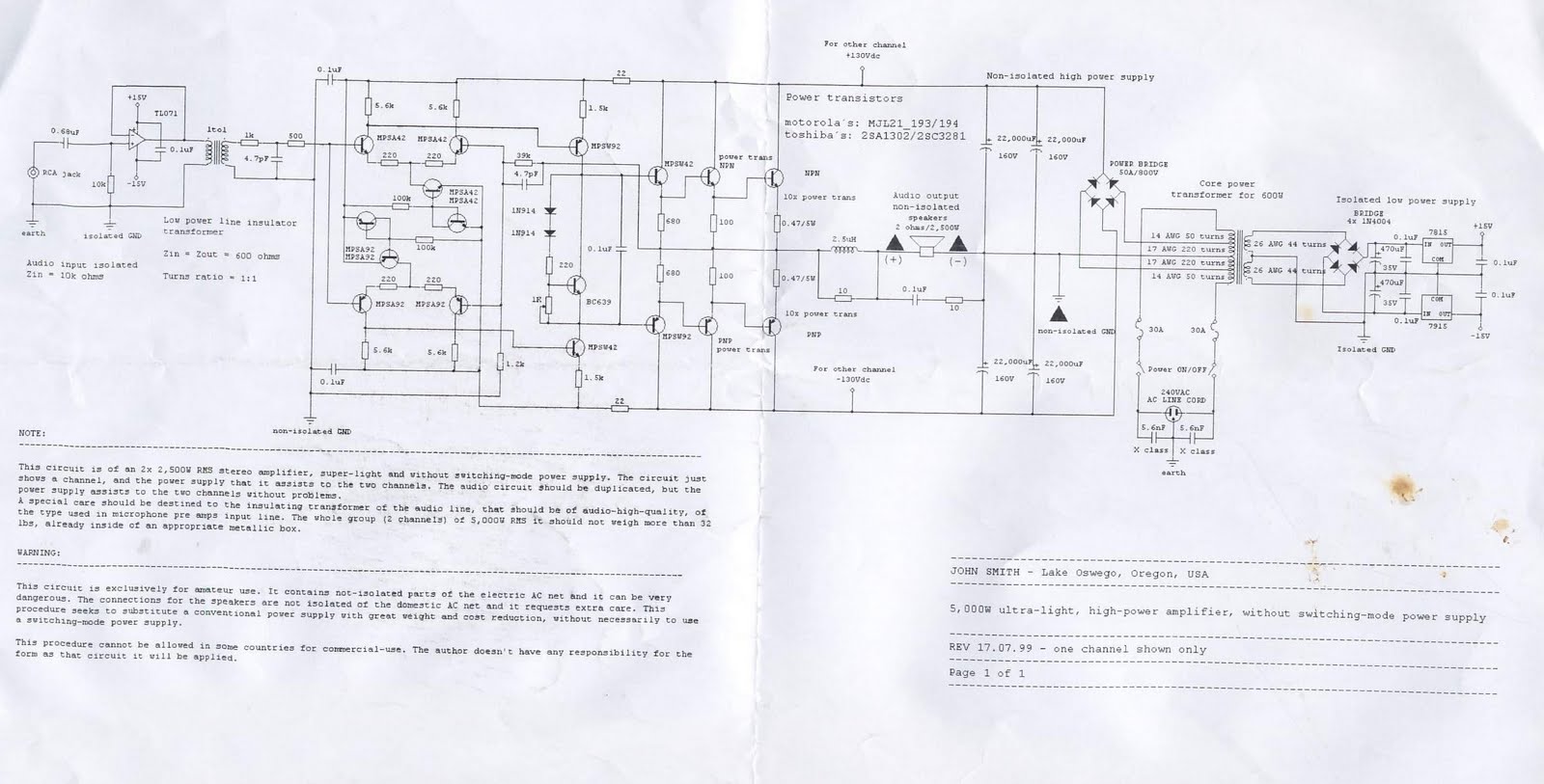
This device is a 2x2, 500W RMS stereo amplifier, designed to be super-lightweight and equipped with a switching-mode power supply. The device features a single channel display and specifies the power output it provides to both channels. The audio...