
Medium-power-inverter
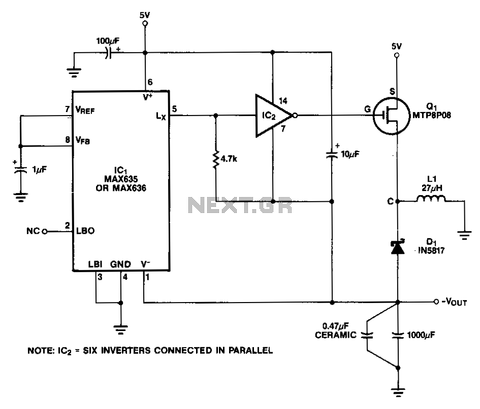
In this circuit, a CMOS inverter, such as the CD4069, is utilized to convert the open-drain Lx output into a signal that is appropriate for driving the gate of an external P-channel MOSFET. The MTP8P03 has a gate threshold voltage ranging from 2.0 V to 4.5 V, resulting in relatively high resistance when driven with only 5 V at the gate. To enhance the gate drive voltage and thus improve efficiency and power handling capability, the negative supply pin of the CMOS inverter is connected to the negative output instead of ground. Once the circuit is powered on, the gate drive for the P MOSFET oscillates between +5 V and -Vout. At startup, -Vout is approximately one Schottky diode drop above ground, and the gate drive to the power MOSFET is slightly less than 5 V. The output should be lightly loaded to ensure proper startup, as the output power capability of the circuit remains very low until -Vout reaches a couple of volts. This circuit generates complementary output signals at frequencies ranging from 50 to 240 Hz. Digital timing control guarantees a separation of 10 to 15 degrees between the fall time of one output and the rise time of the complementary output. The digital section of inverters U1 to U4 manages the drive to Q1 and Q2, both of which are MTE60N20 TMOS devices. These devices are activated alternately with a 11.25-degree separation between complementary outputs. A +12 V supply for CMOS gates U1 to U4 is produced by T1, D3, D4, C7, and U6. The power supply for the TMOS frequency generator is sourced from the diode bridge U5 and capacitor C7, which is applied to the center tap of T2.
The circuit design involves critical components and configurations that enhance its operational reliability and efficiency. The CD4069 CMOS inverter serves as the primary signal conditioning element, converting the open-drain output to a suitable level for the P-channel MOSFET. The choice of the MTP8P03 MOSFET is significant due to its gate threshold voltage characteristics, allowing for effective switching even at lower gate voltages. By connecting the negative supply of the CMOS inverter to the negative output, the circuit achieves a higher effective gate drive voltage, which is essential for driving the P-channel MOSFET efficiently.
The startup conditions are carefully managed, as indicated by the requirement for a lightly loaded output. During startup, the circuit's output power capability is limited, necessitating a cautious approach to loading until the negative output voltage stabilizes. The generation of complementary output signals at variable frequencies is managed by precise timing control, ensuring that the outputs are well-synchronized for optimal performance. The digital control logic ensures that the transitions between outputs are smooth and that there is minimal overlap, enhancing the stability of the circuit.
The power supply architecture is also noteworthy, with T1, D3, D4, C7, and U6 forming a robust power supply for the CMOS gates, ensuring that they function correctly at all times. The diode bridge U5, along with capacitor C7, provides a stable power supply for the TMOS frequency generator, which is critical for maintaining the performance of the circuit under varying load conditions. Overall, the circuit's design reflects a well-thought-out approach to managing power, efficiency, and signal integrity in electronic applications.In this circuit, a CMOS inverter, such as the CD4069, is used to convert the open drain Lx output to a signal suitable for driving the gate of an external P MOSFET. The MTP8P03 has a gate threshold voltage of 2.0 V to 4.5 V, so it will have a relatively high resistance if driven with only 5 V of gate drive.
To increase the gate drive voltage, and thereby increase efficiency and power handling capability, the negative supply pin of the CMOS inverter is connected to the negative output, rather than to ground. Once the circuit is started, the P MOSFET gate drive swings from +5 V to -Vour· At start up, the -Vour is one Schottky diode drop above ground and the gate drive to the power MOSFET is slightly less than 5 V.
The output should be only lightly loaded to ensure start up, since the output power capability of the circuit is very low until -VoUT is a couple of vults. This circuit generates complementary output signals from 50 to 240 Hz. Digital timing control ensures a separation oflO to 15° between the fall time of one output and the rise time of the complementary output.
The digital portion of inverter Ul to U4 controls the drive to Q1 and Q2, both MTE60N20 TMOS devices. These devices are turned on alternately with 11.25° separation between complementary outputs. A +12-V supply for CMOS gates U1 to U4 is developed by T1, D3, D4, C7, and U6. The power supply for the TMOS frequency generator is derived from the diode bridge, U5, and capacitor C7; it is applied to the center tap of T2.
🔗 External reference