Memory Devices
1. Definition and Purpose of Memory Devices
Definition and Purpose of Memory Devices
Memory devices are electronic components designed to store, retain, and retrieve digital or analog data in computing and electronic systems. Their primary function is to provide temporary or permanent storage for instructions and data required by processors, ensuring efficient operation of computational tasks. Memory devices are classified based on volatility, access methods, and underlying technology, each serving distinct roles in system architecture.
Fundamental Characteristics
The performance of memory devices is quantified by three key metrics:
- Access Time (tA): The delay between a read/write request and data availability, typically measured in nanoseconds (ns) for volatile memory and microseconds (µs) for non-volatile variants.
- Data Retention: Volatile memories (e.g., DRAM) lose data without power, while non-volatile memories (e.g., NAND Flash) retain information for years.
- Endurance: The maximum number of write cycles before failure, ranging from 105 cycles for Flash memory to theoretically infinite for SRAM.
where tCL is CAS latency, tRCD is RAS-to-CAS delay, and tRP is row precharge time in synchronous DRAM architectures.
Hierarchy in Computing Systems
Modern systems employ a memory hierarchy to balance speed, capacity, and cost:
Physical Implementation
Memory devices exploit various physical phenomena for data storage:
- Charge Storage: Floating-gate transistors in Flash memory trap electrons to represent binary states
- Magnetic Orientation: Spin-transfer torque MRAM uses electron spin alignment
- Phase Change: Chalcogenide glass transitions between crystalline/amorphous states in PCRAM
- Ferroelectric Polarization: FeRAM utilizes reversible electric dipole moments
where Q is stored charge, Cox is oxide capacitance, VFG is floating gate voltage, and VTH is threshold voltage in Flash memory cells.
Emerging Technologies
Research frontiers include resistive RAM (ReRAM) utilizing filament formation in metal oxides, with switching characteristics described by:
where I0 is pre-exponential factor, Ea is activation energy, and n is ideality factor.
Key Characteristics: Speed, Volatility, and Capacity
Speed: Latency and Throughput
The performance of memory devices is primarily characterized by access time (latency) and bandwidth (throughput). Access time, denoted as tACC, is the delay between a read/write request and data availability. For DRAM, typical access times range from 30–50 ns, while SRAM achieves sub-10 ns due to its static cell design. Bandwidth, measured in GB/s, depends on the interface width and clock frequency. For instance, GDDR6X achieves 1 TB/s via a 384-bit bus at 21 Gbps/pin.
Non-volatile memories like NAND Flash exhibit asymmetric speeds: writes (∼100 μs) are slower than reads (∼25 μs) due to charge tunneling mechanics. Emerging technologies like 3D XPoint reduce this gap with 10 μs access times.
Volatility: Data Retention Mechanisms
Volatility defines whether data persists without power. SRAM and DRAM are volatile, relying on active refresh (DRAM) or static biasing (SRAM). DRAM refresh cycles (∼64 ms) introduce overhead, quantified as:
Non-volatile memories (NVM) like Flash, MRAM, and ReRAM retain data via physical states: trapped charges (Flash), magnetic tunneling junctions (MRAM), or resistive switching (ReRAM). Ferroelectric RAM (FeRAM) uses polarization hysteresis, offering µs-level writes with 1012 endurance cycles.
Capacity: Density and Scaling Limits
Memory capacity scales with cell size and array efficiency. DRAM achieves ∼0.0015 μm2/cell at 15 nm nodes, while 3D NAND stacks 176 layers to reach 1 Tb/die. The theoretical limit for charge-based memories is:
where Q is the minimum detectable charge, C is cell capacitance, and ΔV is sense margin. Below 10 nm, quantum tunneling and variability necessitate error-correction codes (ECC) or multi-level cells (MLC).
Trade-offs and Optimization
- Speed vs. Density: SRAM’s 6T cell prioritizes speed over density, while DRAM’s 1T1C balances both.
- Volatility vs. Power: NVMs eliminate refresh power but incur higher write energy (e.g., NAND at 10 pJ/bit vs. DRAM at 1 pJ/bit).
- Endurance: Flash wears out after 104–105 cycles, whereas ReRAM exceeds 1012 cycles.
Hybrid memory systems (e.g., Optane + DRAM) exploit these trade-offs, placing frequently accessed data in fast volatile tiers and archival data in high-capacity NVMs.
1.3 Classification of Memory Devices
Memory devices are broadly classified based on volatility, access method, and storage technology. Each classification impacts performance metrics such as latency, endurance, and power consumption, making the choice of memory architecture critical in system design.
Volatility-Based Classification
Volatile memory loses stored data when power is removed, while non-volatile memory retains data indefinitely. The underlying physics of these behaviors stems from charge retention mechanisms:
- Volatile Memory (e.g., SRAM, DRAM): Relies on active charge replenishment. DRAM cells store charge on a capacitor, requiring periodic refresh (typically every 64 ms) due to leakage currents governed by:
$$ \tau = RC $$where R is the parasitic resistance and C the storage capacitance. Leakage current follows the Shockley diode equation:$$ I_{leak} = I_0(e^{V_D/nV_T} - 1) $$
- Non-Volatile Memory (e.g., NAND Flash, MRAM): Uses physical state changes. Flash memory traps electrons in a floating gate, with retention times exceeding 10 years. The Fowler-Nordheim tunneling current for programming is:
$$ J = CE_{ox}^2 e^{-B/E_{ox}} $$where Eox is the oxide field and C, B are material constants.
Access Method Classification
Memory access patterns define architectural trade-offs:
- Random Access (RAM): Uniform access latency (typically 10–100 ns) via row/column decoders. Address decoding is implemented with CMOS logic gates, where access time scales as:
$$ t_{acc} = t_{precharge} + t_{decode} + t_{sense} $$
- Sequential Access (Magnetic Tape, CCD): Access time depends on physical location, with seek times following:
$$ t_{seek} = k \cdot \Delta track $$
- Content-Addressable (CAM): Parallel search operations compare stored data with input patterns in a single clock cycle, using XOR-based match circuits.
Storage Technology Classification
Modern memory technologies exploit diverse physical phenomena:
Charge-Based Storage
- DRAM: 1T1C cell with ~30fF storage capacitance. Scaling challenges include maintaining signal-to-noise ratio as capacitance decreases.
- NAND Flash: Multi-level cells (MLC) store 2+ bits/cell by quantizing threshold voltage (Vth). The read margin between states is:
$$ \Delta V_{th} = \frac{V_{max} - V_{min}}{2^n - 1} $$
Spin-Based Storage
- MRAM: Uses magnetic tunnel junctions (MTJs) with tunneling magnetoresistance (TMR) ratios exceeding 300%. The resistance difference between parallel/anti-parallel states is:
$$ \frac{\Delta R}{R} = \frac{2P_1P_2}{1 - P_1P_2} $$where P is the spin polarization.
Phase-Change Memory (PCM)
Exploits resistivity differences between amorphous (high-resistance) and crystalline (low-resistance) phases of chalcogenide glasses. The crystallization kinetics follow Arrhenius behavior:
Emerging Technologies
Research-stage memories include:
- ReRAM: Filamentary switching via ionic motion with switching voltages <1V.
- FeFET: Ferroelectric polarization states with endurance >1012 cycles.
- Optical Memories: Using photonic crystals with picosecond-scale switching.
2. Static RAM (SRAM): Operation and Applications
2.1 Static RAM (SRAM): Operation and Applications
Basic Structure and Operation
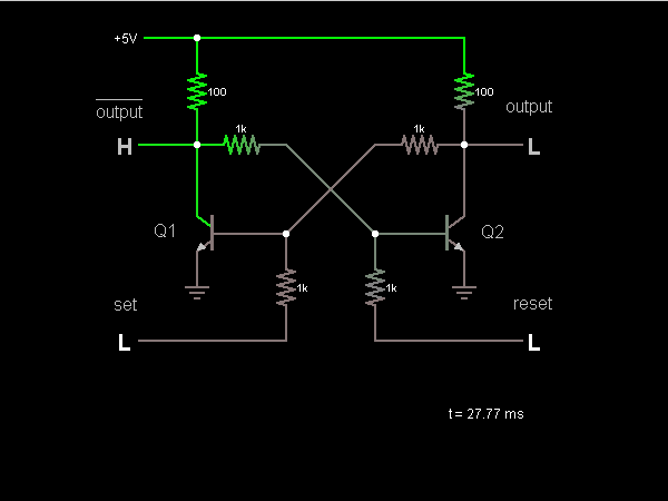
Static RAM (SRAM) stores data using a bistable latching circuit, typically implemented with six transistors per memory cell (6T cell). The core of an SRAM cell consists of two cross-coupled inverters forming a positive feedback loop, ensuring stable state retention as long as power is supplied. Two additional access transistors control read/write operations via the word line (WL) and bit lines (BL, BLB).
The stability of an SRAM cell is quantified by the static noise margin (SNM), which represents the maximum noise voltage that can be tolerated without flipping the stored state. SNM is derived from the voltage transfer characteristics (VTC) of the cross-coupled inverters:
where \( V_{M1} \) and \( V_{M2} \) are the metastable points where the inverter characteristics intersect.
Read and Write Operations
During a read operation, the word line is activated, enabling the access transistors. The bit lines are precharged to \( V_{DD} \), and the cell discharges one bit line through the conducting path of the inverter, creating a voltage differential detected by sense amplifiers.
A write operation requires overpowering the cell's feedback loop. The bit lines are driven to complementary voltages (0 and \( V_{DD} \)), forcing the cell into the desired state. The write margin (WM) defines the minimum bit line voltage required for a successful write:
Performance Characteristics
SRAM offers superior speed compared to DRAM, with access times typically below 10 ns in modern CMOS processes. Key performance metrics include:
- Access time: Delay between address input and data output stabilization
- Cycle time: Minimum time between consecutive operations
- Standby power: Leakage current in idle state (subthreshold and gate leakage)
- Dynamic power: \( P_{dyn} = \alpha C V_{DD}^2 f \), where \( \alpha \) is activity factor
Advanced SRAM Architectures
Modern SRAM designs employ several techniques to improve density and power efficiency:
- 8T and 10T cells: Additional transistors for improved read stability or write ability
- Dual-port SRAM: Independent read/write ports for simultaneous access
- TCAM (Ternary CAM): Content-addressable memory with "don't care" states
Practical Applications
SRAM's speed makes it ideal for applications where latency is critical:
- CPU caches: L1-L3 caches in modern processors (e.g., Intel's Smart Cache)
- Network buffers: High-speed packet buffering in routers and switches
- FPGA configuration memory: Stores programmable logic interconnects
- Space systems: Radiation-hardened SRAM for satellite electronics
Emerging Technologies
Research continues on novel SRAM implementations:
- STT-MRAM: Spin-transfer torque magnetic RAM with non-volatility
- RRAM-based SRAM: Using resistive switching elements for reduced leakage
- 3D SRAM: Monolithic stacking of memory layers for increased density
Dynamic RAM (DRAM): Structure and Refresh Mechanisms
Basic Structure of DRAM
Dynamic RAM (DRAM) stores each bit of data in a separate capacitor within an integrated circuit. The capacitor's charge state (high or low) determines the stored bit value (1 or 0). Unlike SRAM, which uses flip-flops, DRAM's simplicity allows for higher density but requires periodic refreshing due to charge leakage.
A single DRAM cell consists of:
- One access transistor (typically a MOSFET)
- One storage capacitor (usually in the range of 10-30 fF)
The small capacitance value leads to rapid charge leakage, necessitating refresh cycles. The access transistor acts as a switch, controlling charge transfer to and from the capacitor during read/write operations.
DRAM Array Organization
DRAM cells are organized in a grid pattern of rows and columns to minimize address line requirements. A typical architecture uses:
where R is the number of row address bits and C is the number of column address bits. Modern DRAM chips employ bank partitioning to improve parallelism and reduce access latency.
Refresh Mechanisms
DRAM requires periodic refreshing to maintain data integrity. Two primary refresh methods are employed:
1. RAS-Only Refresh (ROR)
In this method:
- Row Address Strobe (RAS) is activated while keeping Column Address Strobe (CAS) high
- An entire row is refreshed at once
- Refresh interval is determined by:
where tREFI is the refresh interval (typically 64 ms) and Nrows is the number of rows.
2. CAS Before RAS Refresh (CBR)
This self-refresh mode:
- Uses an internal counter to cycle through rows
- Reduces power consumption during standby
- Is controlled by the memory controller
Refresh Timing Constraints
The refresh operation imposes timing constraints on DRAM access. The refresh cycle time (tRC) must satisfy:
where tRAS is the Row Address Strobe time and tRP is the Row Precharge time. Modern DDR4 DRAM typically has tRC values between 45-55 ns.
Advanced Refresh Techniques
To address scaling challenges, several advanced refresh techniques have been developed:
- Temperature Compensated Refresh (TCR): Adjusts refresh rate based on junction temperature
- Partial Array Self Refresh (PASR): Refreshes only active memory sections
- Fine Granularity Refresh (FGR): Distributes refresh operations more evenly
These techniques help mitigate the increasing refresh overhead in high-density DRAM while maintaining data retention.
Practical Considerations
In modern systems, DRAM refresh accounts for a significant portion of power consumption. For a 8Gb DDR4 device:
where VDD is the supply voltage (typically 1.2V) and IDD5B is the background current during refresh. This power consideration is crucial for mobile and low-power applications.
2.3 Comparison of SRAM and DRAM
Structural Differences
SRAM (Static Random-Access Memory) stores each bit using a six-transistor (6T) cell, consisting of two cross-coupled inverters and two access transistors. This bistable latching configuration ensures data retention as long as power is supplied, eliminating the need for periodic refresh cycles. The cell's stability comes at the cost of higher area per bit, typically requiring 140–180F² (where F is the feature size). In contrast, DRAM (Dynamic Random-Access Memory) uses a one-transistor-one-capacitor (1T1C) cell, where data is stored as charge on a capacitor. The capacitor's leakage necessitates periodic refreshing (every ~64 ms), but the cell size is significantly smaller (~6–8F²), enabling higher densities.
Performance Metrics
SRAM exhibits faster access times (1–10 ns) due to its static nature and direct read/write paths, making it ideal for CPU caches (L1, L2, L3). DRAM access times are slower (30–100 ns) because of charge sensing and amplification requirements. However, DRAM's burst transfer rates (e.g., DDR5 at 6.4 GT/s) compensate for latency in high-throughput applications. The energy per access also differs: SRAM consumes ~1–10 pJ/bit for active operations, while DRAM requires ~10–100 pJ/bit due to refresh overhead and sense-amplifier activation.
Volatility and Refresh Mechanisms
SRAM is volatile but refresh-free, with data persistence tied directly to power supply integrity. DRAM's volatility stems from capacitor leakage, governed by the refresh current Irefresh:
where C is the cell capacitance, and ΔV is the tolerable voltage drop before data corruption. For a typical 30 fF DRAM cell with ΔV = 0.5 V and Δt = 64 ms, the refresh current per cell is ~0.23 pA. This aggregates to significant power in high-density arrays (e.g., 8 GB DRAM consumes ~100–200 mW for refresh).
Error Modes and Reliability
SRAM suffers from soft errors due to alpha-particle strikes, quantified by the Static Cross Section (SCS):
where Qc is the critical charge to flip a bit, and σ0 is the intrinsic cross-section. DRAM is more susceptible to row hammering, where rapid row accesses induce charge redistribution in adjacent cells. Error-correction codes (ECC) are mandatory for DRAM in critical systems, while SRAM caches often use parity bits or SECDED (Single Error Correction, Double Error Detection).
Applications and Trade-offs
- SRAM: Used in high-speed buffers (CPU caches, register files), FPGAs, and IoT edge devices where latency and power predictability are critical. Its area inefficiency limits use in bulk storage.
- DRAM: Dominates main memory (DIMMs, GDDR for GPUs) and mobile devices (LPDDR) due to its density advantage. Emerging technologies like HBM (High Bandwidth Memory) stack DRAM dies for bandwidth scaling.
Emerging Technologies
Non-volatile alternatives (e.g., MRAM, ReRAM) aim to bridge the SRAM-DRAM gap, but neither matches SRAM's speed or DRAM's cost-per-bit. Hybrid memory cubes (HMC) integrate DRAM with logic dies to mitigate latency through 3D stacking, while SRAM caches evolve with FinFET and GAA (Gate-All-Around) transistors to reduce leakage at advanced nodes (5 nm and below).
3. Read-Only Memory (ROM): Types and Uses
Read-Only Memory (ROM): Types and Uses
Fundamentals of ROM
Read-Only Memory (ROM) is a non-volatile storage medium where data is permanently written during manufacturing or programming. Unlike Random-Access Memory (RAM), ROM retains its contents even when power is removed, making it ideal for firmware, bootloaders, and embedded systems where data persistence is critical. The fundamental operation of ROM relies on a fixed array of memory cells, each storing a binary value (0 or 1) through hardwired connections or programmable elements.
Types of ROM
ROM technology has evolved significantly, leading to several variants with distinct programming mechanisms and applications:
Mask ROM (MROM)
Mask ROM is programmed during semiconductor fabrication using a photomask. Data is permanently encoded in the silicon structure, making it immutable post-production. The memory cell structure consists of a transistor matrix, where the presence or absence of a transistor connection determines the stored bit. The density of MROM is given by:
where A is the chip area, k is a process-dependent constant, and F is the feature size. MROM is cost-effective for high-volume production but lacks flexibility.
Programmable ROM (PROM)
PROM allows post-fabrication programming via fusible links or anti-fuses. A high-voltage pulse is applied to selectively burn out links, creating an open circuit (logical 0) or leaving them intact (logical 1). PROM offers one-time programmability (OTP) and is commonly used in prototyping and low-volume applications.
Erasable PROM (EPROM)
EPROM uses floating-gate transistors for data storage. Charge trapping on the floating gate alters the threshold voltage (Vth), representing a stored bit. EPROM can be erased via ultraviolet (UV) light exposure, which excites trapped electrons and discharges the gate. The erasure process follows the exponential decay model:
where Q(t) is the remaining charge, Q0 is the initial charge, and τ is the UV exposure time constant.
Electrically Erasable PROM (EEPROM)
EEPROM enables byte-level erasure and reprogramming via Fowler-Nordheim tunneling or hot-carrier injection. A control gate modulates the floating gate's charge, allowing precise write/erase cycles. The endurance of EEPROM is typically 104–106 cycles, limited by oxide degradation. The tunneling current density J is given by:
where E is the electric field, and A, B are material-dependent constants.
Flash Memory
Flash memory is a high-density variant of EEPROM that operates on block-level erasure. NAND Flash employs a serial architecture for compact storage, while NOR Flash offers random access for execute-in-place (XIP) applications. The cell threshold voltage distribution is critical for multi-level cell (MLC) and triple-level cell (TLC) designs, where:
Here, q is the electron charge, and Cpp is the inter-poly capacitance.
Applications and Practical Considerations
ROM variants are selected based on access speed, endurance, and cost constraints:
- MROM: Used in mass-produced devices like game cartridges and microcontrollers with fixed firmware.
- PROM: Employed in aerospace and military systems requiring radiation-hardened OTP memory.
- EPROM: Found in legacy industrial systems where field reprogramming is rare but necessary.
- EEPROM: Utilized for configuration storage in IoT devices and BIOS settings.
- Flash: Dominates solid-state drives (SSDs), USB drives, and embedded systems due to its scalability.
Emerging technologies like Resistive RAM (ReRAM) and Phase-Change Memory (PCM) are challenging traditional ROM in applications requiring higher endurance and faster write speeds.
Flash Memory: NAND vs. NOR Architectures
Structural Differences
NAND and NOR flash memories derive their names from the underlying logic gate structures used in their memory cell arrays. In NOR flash, each memory cell is connected directly to a bit line and a word line, enabling random access similar to a NOR logic gate. This architecture allows for byte-level read/write operations, making it ideal for execute-in-place (XIP) applications like firmware storage. In contrast, NAND flash arranges cells in series, resembling a NAND logic gate, which reduces the number of contacts per cell but requires page-level access (typically 4–16 KB). This design trades random access for higher density and lower cost per bit.
Performance Characteristics
The access time for NOR flash is deterministic (<50 ns for reads), as individual cells are addressable. However, write and erase operations are slow (~1 ms per byte) due to the high voltage required for Fowler-Nordheim tunneling. NAND flash, while slower for random reads (~10–50 µs), excels in sequential throughput (up to 1.6 GB/s in modern 3D NAND) due to its page-based access. Erase times are also faster (~2 ms per block, typically 128–256 KB).
Where \( t_{write} \) is the programming time, \( V_{pp} \) is the programming voltage, and \( V_{th} \) is the threshold voltage. The logarithmic dependence highlights the trade-off between speed and voltage stress in floating-gate transistors.
Endurance and Reliability
NOR flash typically endures 100K–1M program/erase (P/E) cycles due to its single-level cell (SLC) dominance, while NAND ranges from 1K (QLC) to 100K (SLC) cycles. Error correction (ECC) is critical for NAND due to higher bit error rates from cell-to-cell interference. Advanced NAND employs wear leveling and over-provisioning to mitigate this.
Applications
- NOR: Embedded systems (MCU firmware), aerospace (radiation-hardened variants), and low-latency read applications.
- NAND: Mass storage (SSDs, USB drives), where density and cost-per-bit outweigh access granularity.
Emerging Technologies
3D NAND stacks cells vertically (e.g., 176 layers in 2023) to overcome planar scaling limits, while NOR evolves with NOR-like MRAM for persistent memory. The energy per bit for NAND continues to decrease following:
Where \( C_{cell} \) is the cell capacitance and \( N_{layers} \) is the 3D stack count.
3.3 Emerging Non-Volatile Memories: MRAM and ReRAM
Magnetoresistive Random-Access Memory (MRAM)
MRAM leverages the tunneling magnetoresistance (TMR) effect to store data in magnetic tunnel junctions (MTJs). An MTJ consists of two ferromagnetic layers separated by a thin insulating barrier. The relative magnetization alignment of these layers determines the junction's resistance:
where θ is the angle between magnetization vectors, R0 is the base resistance, and TMR is the tunneling magnetoresistance ratio. Parallel alignment yields low resistance (logical "0"), while antiparallel alignment produces high resistance (logical "1").
Modern MRAM implementations use spin-transfer torque (STT) switching, where a spin-polarized current directly flips the magnetization of the free layer. The critical current density for switching is given by:
where α is the damping constant, Ms is saturation magnetization, tF is free layer thickness, η is spin polarization efficiency, and Hk is anisotropy field.
Resistive Random-Access Memory (ReRAM)
ReRAM operates through resistive switching in metal-insulator-metal (MIM) structures. The switching mechanism involves formation and rupture of conductive filaments in the dielectric layer. Two primary modes exist:
- Unipolar switching: Set/reset operations use the same voltage polarity but different current magnitudes
- Bipolar switching: Set/reset require opposite voltage polarities
The switching kinetics follow an exponential voltage-time relationship:
where t0 is characteristic time, V0 is activation voltage, and V is applied voltage. The current-voltage characteristics typically show hysteresis:
Comparative Performance Metrics
| Parameter | MRAM | ReRAM |
|---|---|---|
| Switching speed | 1-10 ns | 10-100 ns |
| Endurance | 1015 cycles | 106-1012 cycles |
| Retention | >10 years | >10 years |
| Write energy (pJ/bit) | 0.1-1 | 0.01-0.1 |
Applications and Challenges
MRAM finds use in aerospace and automotive systems due to radiation hardness, while ReRAM shows promise for neuromorphic computing owing to analog resistance states. Key challenges include:
- MRAM: Achieving high TMR ratios (>200%) at low resistance-area products
- ReRAM: Controlling filament formation for uniform switching characteristics
- Both: Scaling below 10 nm while maintaining performance
Recent advances include voltage-controlled magnetic anisotropy MRAM for lower power operation and oxide engineering in ReRAM for improved uniformity.
4. Cache Memory: Levels and Mapping Techniques
4.1 Cache Memory: Levels and Mapping Techniques
Cache memory serves as a high-speed buffer between the CPU and main memory, reducing latency by storing frequently accessed data. Its performance is governed by hierarchical organization and mapping techniques, which determine how data is stored and retrieved.
Cache Hierarchy
Modern processors employ a multi-level cache hierarchy to balance speed and capacity:
- L1 Cache (Level 1): The smallest (typically 8–64 KB) and fastest, split into instruction and data caches. Access latency is 1–4 cycles.
- L2 Cache (Level 2): Larger (256 KB–8 MB) with higher latency (10–20 cycles). Often shared between cores in multi-core processors.
- L3 Cache (Level 3): The largest (8–64 MB) and slowest (30–50 cycles), shared across all cores to minimize main memory accesses.
The inclusive property ensures data in L1 is also present in L2/L3, while exclusive designs avoid redundancy. Intel’s Smart Cache and AMD’s Infinity Fabric leverage these hierarchies for optimal throughput.
Cache Mapping Techniques
Mapping techniques define how main memory blocks are allocated to cache lines. The three primary methods are:
Direct Mapping
Each memory block maps to exactly one cache line, determined by:
While simple, this leads to high conflict misses when multiple blocks compete for the same line. For example, a 32 KB cache with 64-byte lines has 512 lines. Address 0x1200 maps to line (0x1200 / 64) mod 512.
Fully Associative Mapping
A memory block can occupy any cache line, eliminating conflicts but requiring complex parallel search hardware (Content-Addressable Memory). The tag comparison checks all lines simultaneously:
Practical for small caches (e.g., TLB), but prohibitive for larger sizes due to O(n) search complexity.
Set-Associative Mapping
A compromise between direct and fully associative designs. The cache is divided into sets, each containing n ways (typically 2–16). The set index is computed as:
Within a set, any way can store the block. A 4-way associative 32 KB cache with 64-byte lines has 128 sets (512 lines / 4 ways). Intel’s CPUs commonly use 8–12-way associativity for L2/L3 caches.
Replacement Policies
For associative caches, replacement policies determine which line to evict:
- Least Recently Used (LRU): Evicts the least recently accessed line, optimal but hardware-intensive.
- Random: Simple but unpredictable performance.
- Pseudo-LRU: Approximates LRU with lower overhead, used in ARM Cortex and x86 architectures.
Real-world implementations often combine policies. For instance, Intel’s L3 cache uses a dynamic insertion policy to balance thrashing and fairness.
Write Policies
Cache coherence is maintained through write policies:
- Write-Through: Data is written to both cache and main memory simultaneously, ensuring consistency but increasing latency.
- Write-Back: Data is written only to cache, with main memory updated later (on eviction). Faster but requires dirty-bit tracking.
Modern processors employ write-back for L1/L2 caches, with write-combining buffers to optimize burst writes to memory.
Case Study: AMD Zen 4 Cache Architecture
AMD’s Zen 4 features a unified L3 cache (up to 64 MB) with a 16-way associative design. Each core has a private 1 MB L2 cache (8-way associative), while L1 (32 KB instruction + 32 KB data) uses 8-way associativity. The Infinity Fabric interconnects these caches at 32 bytes/cycle, reducing inter-core latency.
4.2 Virtual Memory and Paging
Concept and Architecture
Virtual memory decouples logical address spaces from physical memory, allowing processes to operate as if they have access to a contiguous, large memory space. This abstraction is achieved through paging, where memory is divided into fixed-size blocks called pages (typically 4 KB in modern systems). The Memory Management Unit (MMU) maps virtual addresses to physical addresses via a page table.
Page Table Structure
Each process maintains a page table, where entries store the mapping between virtual and physical pages. A basic page table entry (PTE) contains:
- Present/Absent bit – Indicates whether the page is in physical memory.
- Frame number – Physical memory location (if present).
- Protection bits – Read/write/execute permissions.
- Modified (Dirty) bit – Tracks whether the page has been altered.
Address Translation
For a 32-bit system with 4 KB pages, the virtual address splits into:
The MMU uses the page number to index the page table, retrieves the frame number, and combines it with the offset to form the physical address:
Translation Lookaside Buffer (TLB)
To mitigate the latency of page table walks, processors use a TLB, a cache storing recent virtual-to-physical mappings. A TLB hit resolves the address in ~1 cycle, while a miss triggers a full page table traversal. The effective memory access time (EAT) is:
Page Faults and Demand Paging
When a referenced page is not in physical memory (page fault), the OS:
- Locates the page on disk (swap space or file system).
- Selects a victim page (using algorithms like LRU or Clock).
- Writes the victim to disk if dirty, then loads the requested page.
This demand paging strategy optimizes memory usage by loading pages only when needed.
Multi-Level Paging
For large address spaces (e.g., 64-bit systems), a single page table would be impractical. Hierarchical paging divides the page number into multiple indices. For example, a two-level scheme splits the 20-bit page number into two 10-bit indices:
Each level points to a sub-table, reducing memory overhead by storing only active subtables.
Real-World Optimizations
Modern systems employ advanced techniques:
- Inverted Page Tables – Store one entry per physical frame, reducing memory usage at the cost of slower lookups.
- Hashed Page Tables – Use hash functions to compactly store mappings.
- Page Table Isolation (PTI) – Mitigates speculative execution vulnerabilities (e.g., Meltdown) by separating kernel and user page tables.
4.3 Memory Access Optimization Strategies
Cache-Aware and Cache-Oblivious Algorithms
Memory access latency is dominated by cache misses, making cache optimization critical. Cache-aware algorithms explicitly account for cache line size (L) and cache capacity (C), while cache-oblivious algorithms achieve optimal performance without prior knowledge of cache parameters. For example, blocked matrix multiplication reduces cache misses by decomposing matrices into sub-blocks of size B × B, where B ≈ √C.
Here, S is stride length, and k is a locality factor. Real-world implementations in numerical libraries (e.g., BLAS) use such blocking to achieve near-peak FLOP/s.
Prefetching Techniques
Hardware and software prefetching mitigate latency by predicting future accesses. Stream-based prefetchers detect sequential patterns, while stride prefetchers track fixed offsets. Advanced CPUs (e.g., Intel’s ADL) use machine learning for prefetch accuracy. A prefetch distance D must satisfy:
Memory-Level Parallelism (MLP)
MLP exploits bank parallelism in DRAM by interleaving requests across channels. The theoretical bandwidth (BW) for N channels is:
In practice, DDR5 achieves ~38.4 GB/s per channel at 4800 MT/s. GPUs leverage MLP aggressively via coalesced memory accesses, reducing transaction overhead.
Data Structure Optimization
Structure-of-Arrays (SoA) outperforms Array-of-Structures (AoS) in SIMD architectures by enabling vectorized loads. For a struct with fields x, y, z, SoA stores x[...], y[...], z[...] contiguously. This improves spatial locality and reduces cache pollution.
Non-Uniform Memory Access (NUMA) Tuning
NUMA systems require thread affinity and data placement policies. First-touch initialization ensures memory allocation near the accessing CPU. Linux’s numactl tool enforces policies like:
- --interleave=all: Distributes pages across nodes
- --preferred=node: Favors a specific node
Compiler Directives and SIMD
#pragma omp simd (OpenMP) and __restrict keywords guide compilers to vectorize loops. For example:
#pragma omp simd
for (int i = 0; i < N; i++) {
    C[i] = A[i] + B[i];
}
This eliminates false dependencies, enabling AVX-512 or NEON instructions.
DRAM Timing Optimization
Reducing tRCD (RAS-to-CAS delay) and tRP (precharge time) improves row buffer hit rates. For a 64ms refresh interval (tREFI), the effective bandwidth loss due to refresh is:
5. Recommended Textbooks and Research Papers
5.1 Recommended Textbooks and Research Papers
- PDF Chapter 5 - Internal Memory - Pacific University — Chapter 5 - Internal Memory Reading: Section 5.1 on pp. 145-154 Memory Basics Early memory was made out of doughnut-shaped ferromagnetic loops called cores; thus, today, main memory is still referred to as core memory. Cache memory is composed of SRAM (static RAM) • faster • more expensive • less dense
- Organic Electronic Memory Devices | Electrical Memory Materials and ... — Extensive studies toward new organic/polymeric materials and device structures have been carried out to demonstrate their unique memory performances. 17-22 This chapter provides an introduction to the basic concepts and history of electronic memory, followed by a brief description of the structures and switching mechanisms of electrical memory devices classified as transistors, capacitors ...
- Memory Devices for Flexible and Neuromorphic Device Applications — Nevertheless, the emerging material-based memory devices have a great potential for the application such as neuromorphic devices, biofriendly devices, and wearable devices. Because research on emerging material-based memory devices is accelerated and rapidly increases, great progress in memory technology will be viable in the near future.
- Semiconductor Memories and Systems - 1st Edition - Elsevier Shop — Andrea Redaelli received the Laurea and Ph.D. degrees in electronic engineering from Politecnico di Milano, Italy, in 2003 and 2007 respectively. ... Redaelli is also the editor of a book titled "Phase Change Memory: device physics, reliability and applications", he is author and co-author of more than 50 papers, and more than 100 patents ...
- PDF Semiconductor Memory Devices and Circuits - api.pageplace.de — The memory hierarchy includes on-chip cache and off-chip standalone memories such as main memory, storage-class-memory, and solid-state drive. This book will introduce the semiconductor memory technologies that serve various levels of the memory hierarchy, from the device cell structures to the array-level design, with an
- PDF Electrical Memory Materials and Devices - api.pageplace.de — followed by a number of application-related examples of organic memory devices. Chapter 3 reports on the use of donor-acceptor structures in resis-tive memory devices. The chapter highlights the importance of structure to property relationships in understanding the switching mechanism and also discusses multilevel resistive memory devices.
- PDF The Memory System UNIT 5 THE MEMORY SYSTEM - eGyanKosh — The cost of per unit of memory increases as you go up in the memory hierarchy i.e. Memory tapes and auxiliary memory are the cheapest and CPU Registers are the costliest amongst the memory types. The amount of data that can be transferred between two consecutive memory layers at a time decreases as you move up in the pyramid. For example, from
- Semiconductor Memory Technologies | SpringerLink — The aim of this chapter of the Handbook of Semiconductor Devices is to illustrate the actual scenario of semiconductor memory technologies; the chapter is organized as follows:. The first section will provide a general introduction to sketch the classes of memory technologies in terms of volatile, nonvolatile, and emerging memories, their fundamental features, and applications.
- Unit - 5 | unit 5 semiconductor memories and programmable logic devices ... — Master the concepts of Unit - 5with detailed notes and resources available at Goseeko. Ideal for students and educators in Information Technology
- Semiconductor Memories and Systems | ScienceDirect — Abstract. In this chapter, the main memory technology from a historical point of view will be presented. Following a chronological line, after the pioneering work exploiting the CMOS technology to build useful memories, first DRAM and then NAND technology will be overviewed, covering at least three decades of the semiconductor memory evolution.
5.2 Online Resources and Datasheets
- Organic Electronic Memory Devices | Electrical Memory Materials and ... — Extensive studies toward new organic/polymeric materials and device structures have been carried out to demonstrate their unique memory performances. 17-22 This chapter provides an introduction to the basic concepts and history of electronic memory, followed by a brief description of the structures and switching mechanisms of electrical memory devices classified as transistors, capacitors ...
- Find Datasheets, Electronic Parts, Components - Datasheets.com — Datasheets.com is the easiest search engine to find datasheets of electronic parts. Search millions of components across thousands of manufacturers. Datasheets. Part Explorer ... EVAL-AD5933EBZ, Evaluation Board Evaluating the AD5933, 1-MSPS, 12-Bit Impedance Converter Network Analyzer by: Analog Devices. Typical Application Circuit for ...
- CS 312, CH 5 Flashcards - Quizlet — Study with Quizlet and memorize flashcards containing terms like 5.1) What are the key properties of semiconductor memory?, 5.2) What are two interpretations of the term random-access memory?, 5.3) What is the difference between DRAM and SRAM in terms of applications? and more.
- ALLDATASHEET.COM - Electronic Parts Datasheet Search — (Analog Devices) MSK5142-1.7HTD ... ALLDATASHEET.COM is the biggest online electronic component datasheets search engine. - Contains over 50 million semiconductor datasheets. - More than 60,000 Datasheets update per month. - More than 460,000 Searches per day. - More than 28,000,000 Impressions per month.
- Electronics Datasheets - Parts Search and Technical Documents — Your Source for Online Electronic Component Datasheets. We give you instant and unrestricted access to a comprehensive resource of datasheets and other technical documents from our growing database of electronics parts, sourced directly from the top global electronics manufacturers.
- PDF The Memory System UNIT 5 THE MEMORY SYSTEM - eGyanKosh — The cost of per unit of memory increases as you go up in the memory hierarchy i.e. Memory tapes and auxiliary memory are the cheapest and CPU Registers are the costliest amongst the memory types. The amount of data that can be transferred between two consecutive memory layers at a time decreases as you move up in the pyramid. For example, from
- PDF Semiconductor Memory Devices and Circuits - api.pageplace.de — access memory (FeRAM) and ferroelectric field-effect transistor (FeFET). The mul-tilevel capability, variability, and reliability issues of eNVM devices will be addressed. Chapter 5 also introduces the concept of the compute-in-memory that merges the mixed-signal computation into the memory arrays for accelerating the v ector-matrix
- Unit 5: Memory Programmable Logic Devices — unit5 - Free download as PDF File (.pdf), Text File (.txt) or read online for free. The document discusses different types of memory used in digital systems, including RAM, ROM, and programmable logic devices. RAM allows random access reading and writing of data but loses its contents when power is removed, while ROM provides permanent data storage that can only be read.
- Unit - 5 | unit 5 semiconductor memories and programmable logic devices ... — Master the concepts of Unit - 5with detailed notes and resources available at Goseeko. Ideal for students and educators in Information Technology
- PDF eMMC Architecture and Operation - CMOSedu.com — ECG 721 -Memory Circuit Design, Spring 2017 Jonathan K DeBoy 1. Overview •Flash memory programming and reading •MultiMedia Card (MMC) •Embedded MMC (eMMC) •Packet Formats & Operation •Future Technologies 2. ... •Developed by Joint Electron Device Engineering Council (JEDEC)
5.3 Advanced Topics for Further Study
- PDF Advanced Memory Technology: Functional Materials and Devices — 4.2 Memory Technologies: Types of Electronic Memory and Memristors 122 4.2.1 Classification of Memristors 123 4.2.2 Current-Voltage (I-V) Characteristics 124 4.3 Noise in Materials and Electronic Devices 125 4.3.1 Johnson-Nyquist (Thermal) Noise 127 4.3.2 Shot Noise 127 4.3.3 Random Telegraph Noise (RTN) 127
- PDF The Memory System UNIT 5 THE MEMORY SYSTEM - eGyanKosh — Various memory devices in a computer system forms a hierarchy of components which can be visualised in a pyramidal structure as shown in Figure 5.2. As you can ... concept is further explained in next unit. In subsequent sections and next unit, we will discuss various types of memories in more detail. 5.3 SRAM, DRAM, ROM, FLASH MEMORY ...
- Organic Electronic Memory Devices | Electrical Memory Materials and ... — Extensive studies toward new organic/polymeric materials and device structures have been carried out to demonstrate their unique memory performances. 17-22 This chapter provides an introduction to the basic concepts and history of electronic memory, followed by a brief description of the structures and switching mechanisms of electrical memory devices classified as transistors, capacitors ...
- CS 312, CH 5 Flashcards - Quizlet — Study with Quizlet and memorize flashcards containing terms like 5.1) What are the key properties of semiconductor memory?, 5.2) What are two interpretations of the term random-access memory?, 5.3) What is the difference between DRAM and SRAM in terms of applications? and more.
- Memory characteristics and mechanisms in transistor-based memories — Memory devices receive and record digital information. They are core components of computers and electronic systems. Electrical memory devices can be classified into two categories based on their need of power: when power is off, volatile memory loses the stored data, while data in nonvolatile memory retains [1].These storage technologies mainly exploit a material's characteristics such as ...
- TestOut Practice Questions (5.1 - 5.3) Flashcards - Quizlet — Chapters 5.1 - 5.3 Learn with flashcards, games, and more — for free.
- High-Density Solid-State Memory Devices and Technologies - MDPI — Electronics, an international, peer-reviewed Open Access journal. ... this Special Issue aims to examine high-density solid-state memory devices and technologies from various standpoints that are relevant to foster their continuous success in the future. In particular, manuscripts are solicited on topics related but not limited to the following ...
- Unit - 5 | unit 5 semiconductor memories and programmable logic devices ... — Master the concepts of Unit - 5with detailed notes and resources available at Goseeko. Ideal for students and educators in Information Technology
- PDF Advanced Memory and Device Packaging - Springer — 2 1 Advanced Memory and Device Packaging. Fig. 1.1 . Bonding wire and applications in memory device packaging . packaging. Au coated Ag wire could be the alternate option of Au wire however it needs further recipe optimization to resolve some workability issues such as short-tailing issue.
- Unit 5: Memory Programmable Logic Devices — The document discusses different types of memory used in digital systems, including RAM, ROM, and programmable logic devices. RAM allows random access reading and writing of data but loses its contents when power is removed, while ROM provides permanent data storage that can only be read. Programmable logic devices like PLDs and PLA can be programmed to implement custom logic functions and ...