
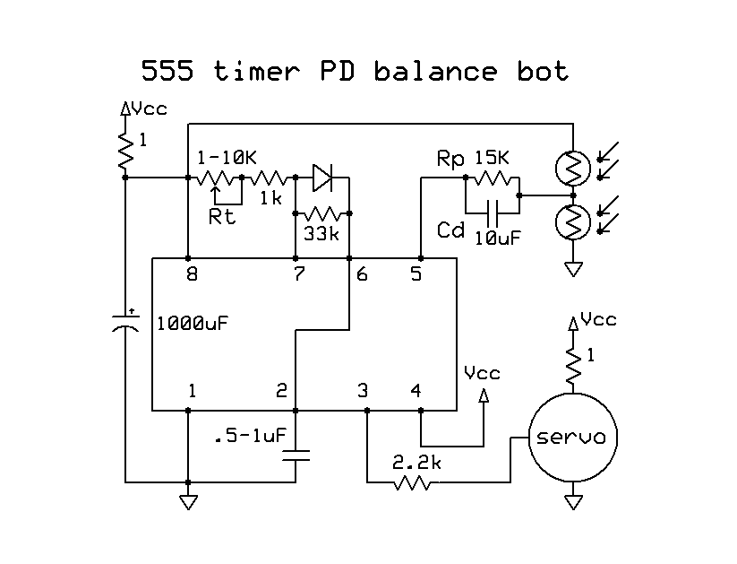
meter schematic diagram
The project entails a comprehensive approach to RF circuit design, necessitating a meticulous schematic layout that accurately reflects the functional requirements of the system. The schematic should detail all components, including the RF amplifier, filters, and any necessary matching networks to ensure optimal performance across the desired frequency range.
The PCB layout must be designed to minimize interference and maintain signal integrity. Key considerations include the placement of components to reduce trace lengths, careful routing of RF paths, and the implementation of ground planes to shield sensitive components. Additionally, the design should facilitate thermal management to prevent overheating of RF components during operation.
The RFOUT coaxial connection will serve as the output interface for the antenna, which should be selected based on the frequency of operation and the gain requirements of the system. Proper impedance matching at this interface is crucial to maximize power transfer and minimize signal reflections.
The CLKOUT coaxial connection may interface with an RF meter, which will provide real-time monitoring of the RF output signal. The design should incorporate appropriate signal conditioning to ensure that the RF meter receives a clean and accurate representation of the output signal.
Documentation generated for the contractor must include detailed schematics, PCB layout files, and a bill of materials (BOM) that lists all components used in the design. Additionally, any relevant testing procedures or performance specifications should be included to guide the contractor in the assembly and validation of the RF circuit.
Ultimately, the project aims to deliver a robust RF design that meets specified performance criteria while adhering to best practices in RF circuit design and PCB layout.The current task is to design the schematic layout, design the PCB layout, and generate the. contractor with RF schematic design and PCB layout experience Please review the block diagram in the attached. antenna will be connected to the RFOUT coax and an RF meter may be connected to the CLKOUT coax. The entire 🔗 External reference
Related Circuits
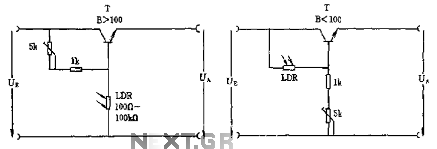
The circuit depicted involves a photoresistor (LDR) connected to a transistor, which operates at either a high or low level based on light conditions. The amplification factor of the transistor is 100, which is adequate for the application. The...
To construct the circuit, follow the provided schematic. If assistance is required, do not hesitate to reach out for support. If there are difficulties in identifying the components... To build the circuit effectively, it is essential to adhere closely to...
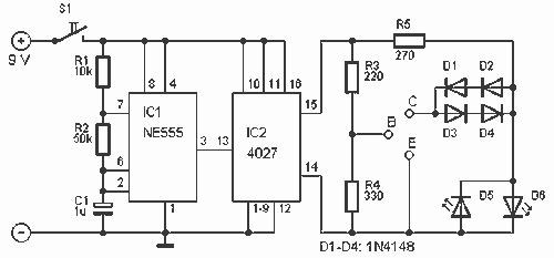
This is a convenient design for a transistor tester. The advantage of this circuit is that transistors can be tested without actually doing the circuit soldering. The tester uses two ICs: an NE 555 timer and a CMOS IC...
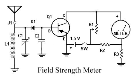
This circuit utilizes a single 1.5V battery. The capacitor C1 must be adjusted for optimal peak reading. To operate the circuit, the transmitter and meter should be turned on. The circuit is designed to operate efficiently with a single 1.5V...

In an audio amplifier, the quality of sound depends on several factors, including the quality of active and passive components, circuit configuration, and layout. The selection of components is influenced by the constructor's budget. Discrete active components like transistors...
A schematic diagram is a layout of symbols and connections representing every electronic component in a circuit, serving as a guide to understanding how the circuit functions. Learning to read these diagrams may initially seem challenging, but it is...
Warning: include(partials/cookie-banner.php): Failed to open stream: Permission denied in /var/www/html/nextgr/view-circuit.php on line 713
Warning: include(): Failed opening 'partials/cookie-banner.php' for inclusion (include_path='.:/usr/share/php') in /var/www/html/nextgr/view-circuit.php on line 713