
Miniature Beeping Circuit
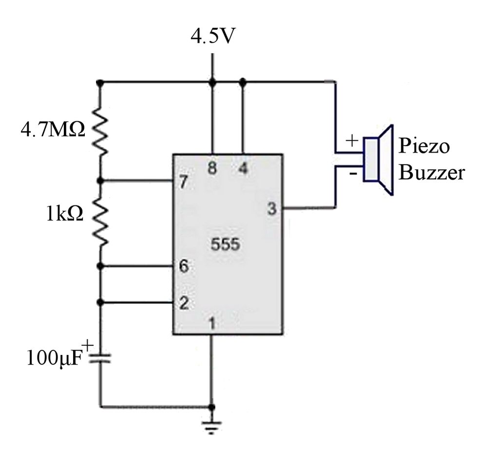
The 555 timer in astable mode operates as an oscillator, producing a continuous square wave output without requiring any external triggering. In this configuration, the circuit consists of a 555 timer IC, resistors, a capacitor, and a buzzer.
The timing components, typically two resistors (R1 and R2) and a capacitor (C1), determine the frequency of the output pulse. The frequency (f) and duty cycle (D) of the output waveform can be calculated using the formulas:
f = 1.44 / ((R1 + 2R2) * C1)
D = (R2 / (R1 + 2R2)) * 100%
Where:
- R1 is connected between the discharge pin (Pin 7) and Vcc (positive supply voltage).
- R2 is connected between the discharge pin (Pin 7) and the threshold pin (Pin 6).
- C1 is connected between the threshold pin (Pin 6) and ground.
The output from the 555 timer is taken from the output pin (Pin 3), which drives the buzzer. The buzzer will sound each time the output pin transitions from low to high, producing an audible beep at the defined intervals.
For practical implementation, it is important to select appropriate resistor and capacitor values to achieve the desired timing characteristics. Additionally, the power supply voltage should be compatible with the 555 timer specifications, typically ranging from 4.5V to 15V.
By adjusting R1, R2, and C1, the circuit can be customized for various applications, such as alarms, timers, or sound indicators, making it a versatile choice for basic timing and sound generation tasks.The circuit is a basic 555 timer circuit in astable mode. In this configuration the IC sends a brief pulse to the buzzer every few minutes. The values.. 🔗 External reference
Related Circuits
The quartz crystal oscillator circuit is highly advantageous in terms of frequency stability. Even the Voltage-Controlled Crystal Oscillator (VCXO) circuit, which allows for significant frequency changes, typically experiences only about a 1% variation. However, the linear range of control...
The circuit operates as an electronic ballast for fluorescent lamps, incorporating a rectifier filter circuit, a high-frequency oscillation circuit, and an output circuit. The rectifier filter circuit consists of a rectifier diode (VD1) and filter capacitors (C1, C2). The...
A P-type transistor (VT2, VT3) and other components form a common emitter-coupled trigger, functioning as a Schmitt trigger device. This setup serves as a switching circuit to detect changes in the resistance of a PTC thermistor, thereby controlling the...
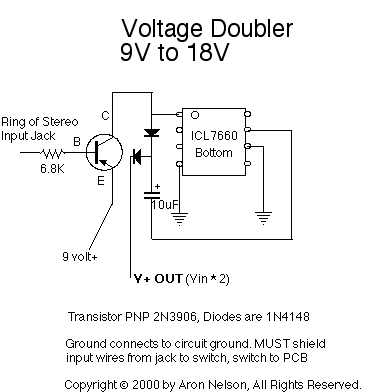
If you want to try a higher voltage with your pedals, try this simple and easy voltage doubler circuit which uses an ICL7660 CMOS Voltage Converter Chip. I have found that JFETs such as the J201 sound much better...
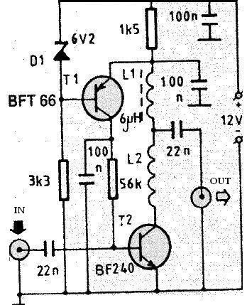
This RF antenna amplifier is designed for high frequency and VHF bands (for radio and TV) and provides a gain of 22 dB. The amplifier features very low noise, measured at under 1.6 dB. The L1 coil has a...
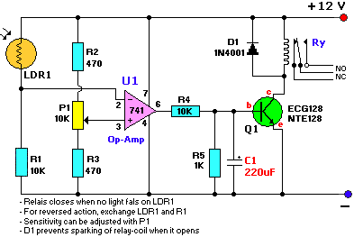
The provided schematic diagram illustrates an LM741 light/dark sensor circuit, derived from the 741 Op-Amp Tutorial by Tony van Roon. The ECG128/NTE128 transistor can be replaced with any NPN transistor that meets the necessary gain and current specifications for...