
Negative Pulse Stretcher
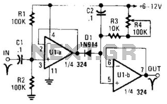
In this circuit, U1A serves as a critical amplification stage, enhancing the signal strength from the input source before it reaches the diode D2 and capacitor C2. The role of D2 is to allow current to flow in one direction, effectively protecting the circuit from reverse polarity and ensuring that C2 is charged appropriately. The capacitor C2 plays a pivotal role in the circuit, storing energy and smoothing out the voltage levels to accommodate different pulse rates.
U1B, designated as a voltage follower, provides high input impedance and low output impedance. This configuration ensures that the voltage at the output follows the voltage at the input without loading the previous stage, making it ideal for buffering signals.
Resistors R3 and R4 are integral to controlling the pulse stretching mechanism. By adjusting their values, the timing characteristics of the circuit can be altered, allowing for fine-tuning of the input pulse's duration before it is processed by the subsequent stages. This flexibility is essential for applications requiring precise timing and pulse width modulation.
Overall, the circuit demonstrates a well-coordinated interaction between amplification, voltage following, and timing control, making it suitable for various electronic applications where pulse shaping and signal integrity are paramount. U1A acts as an amplifier, which drives D2 and charges C2. U1B acts as a voltage follower. R3 and R4 determine the amount of stretch that the input pulse receives. C2 can be charged to accommodate different pulse rates. 🔗 External reference
Related Circuits
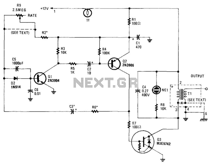
This high-voltage pulse supply generates pulses up to 30 kV. Q1 and Q2 form a multivibrator in conjunction with peripheral components R1 through R6, and C1, C2, C3, C5, C6, and D2. R9 adjusts the pulse repetition rate, while...
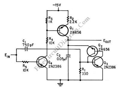
This is a schematic diagram of a pulse width to analog demodulator circuit. This circuit is used to demodulate the pulse width to an analog voltage level. The pulse width to analog demodulator circuit is designed to convert pulse-width modulated...
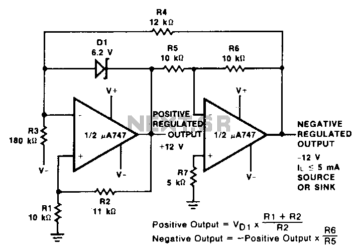
This reference utilizes an operational amplifier (op amp) to generate a negative output voltage that corresponds with the positive reference voltage. A pA747 dual op amp, or any similar device such as an LM1458 or two 1-A741 devices, can...
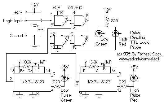
This circuit uses LEDs to display logic states for high, low, rising pulse, and falling pulse. It is generally useful for debugging logic circuitry. The described circuit employs light-emitting diodes (LEDs) as visual indicators for various logic states in digital...
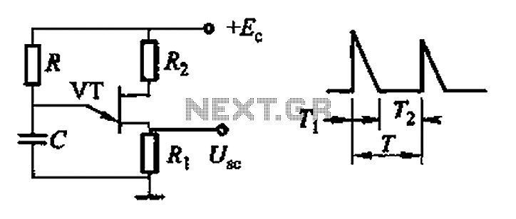
Common non-sinusoidal oscillator circuit, waveform and frequency formula - pulse wave oscillator - blocking oscillator transformer The common non-sinusoidal oscillator circuit is designed to generate pulse waveforms, which are characterized by their square or rectangular shape. These oscillators are...
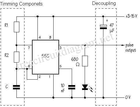
The SE555/NE555 timer was first introduced by the Signetics Corporation around 1971. Pin connections and functions are as follows: Pin 1 (Ground) - This pin serves as the ground or common pin, representing the most negative supply potential of...
Warning: include(partials/cookie-banner.php): Failed to open stream: Permission denied in /var/www/html/nextgr/view-circuit.php on line 713
Warning: include(): Failed opening 'partials/cookie-banner.php' for inclusion (include_path='.:/usr/share/php') in /var/www/html/nextgr/view-circuit.php on line 713