Negative Voltage Regulators
1. Definition and Purpose of Negative Voltage Regulators
Definition and Purpose of Negative Voltage Regulators
A negative voltage regulator is an electronic circuit or integrated device designed to maintain a stable, predefined negative output voltage despite variations in input voltage, load current, or temperature. Unlike positive voltage regulators, which maintain a positive output, negative regulators ensure a consistent negative potential relative to ground or a reference point.
Fundamental Operating Principle
The core function of a negative voltage regulator is governed by feedback control, where the output voltage is compared against a reference voltage. Any deviation triggers corrective action via an error amplifier and pass element (typically a transistor or MOSFET). The regulator adjusts conduction to maintain:
where Vref is the internal reference voltage, and R1, R2 form an external feedback network. Stability is achieved through compensation networks that mitigate phase shifts.
Key Design Parameters
- Line Regulation: Measures the output voltage variation per unit change in input voltage (typically in mV/V or %).
- Load Regulation: Quantifies output stability under varying load currents (expressed in mV/mA or %).
- Dropout Voltage: The minimum required difference between input and output voltages for regulation (e.g., -5V output requires input ≤ -5.5V for a 0.5V dropout).
- Thermal Resistance (θJA): Critical for power dissipation calculations, given by:
where Tj is junction temperature, Ta ambient temperature, and Pd power dissipation.
Practical Applications
Negative voltage regulators are indispensable in systems requiring symmetrical power rails, such as:
- Operational amplifier circuits (±15V supplies)
- Data acquisition systems (e.g., -5V for analog frontends)
- Telecommunication equipment (RS-232 interface requiring ±12V)
Historical context reveals early implementations using discrete zener diodes and bipolar transistors, later supplanted by monolithic ICs like the 79xx series (e.g., 7905 for -5V). Modern designs employ low-dropout (LDO) topologies with PNP or PMOS pass elements to minimize power loss.
Comparative Analysis with Positive Regulators
While operational principles mirror positive regulators, key distinctions include:
- Ground Referencing: Negative regulators reference the output to the positive rail, complicating feedback network design.
- Pass Element Configuration: PNP/NPN or PMOS/NMOS pairings are inverted compared to positive regulators.
- Stability Challenges: Higher output impedance of PNP/PMOS devices necessitates careful compensation.
1.2 Key Characteristics and Specifications
Output Voltage and Line Regulation
The primary function of a negative voltage regulator is to maintain a stable output voltage (VOUT) despite variations in input voltage (VIN) or load current (ILOAD). Line regulation quantifies this stability and is defined as:
For precision applications, high-performance regulators like the LM337 achieve line regulation below 0.01%/V. The output voltage is typically adjustable via external resistors, with the relationship given by:
where VREF is the reference voltage (typically -1.25V) and IADJ is the adjust pin current (~50µA).
Load Regulation and Dropout Voltage
Load regulation measures the output voltage variation under changing load conditions:
where VNL and VFL are no-load and full-load voltages, respectively. Modern regulators maintain load regulation within 1-5mV. The dropout voltage—the minimum required VIN-to-VOUT differential—is critical for low-voltage applications. For example, the LT3015 features a 300mV dropout at 1.5A.
Thermal Performance
Power dissipation (PDISS) is calculated as:
where IQ is the quiescent current. Thermal resistance (θJA) determines junction temperature rise:
For TO-220 packages, θJA typically ranges from 50-65°C/W. Proper heatsinking is essential for high-current applications.
Noise and Ripple Rejection
Negative regulators suppress input noise through power supply rejection ratio (PSRR):
High-performance designs like the ADP7182 achieve >70dB PSRR at 1kHz. External bypass capacitors further enhance noise rejection, with the optimal value often determined by:
where fCROSS is the regulator's crossover frequency.
Protection Features
Advanced negative regulators incorporate:
- Current limiting: Foldback or constant-current schemes protect against shorts
- Thermal shutdown: Typically activates at 150-175°C with hysteresis
- Reverse-bias protection: Essential for battery-backed systems
For example, the MIC29712 implements a ±50V input transient rating with internal ESD protection up to 4kV.
1.3 Comparison with Positive Voltage Regulators
Negative and positive voltage regulators serve complementary roles in power supply design, but their operational principles and applications differ significantly. While both stabilize output voltage, their topologies, grounding schemes, and performance characteristics diverge in ways that influence circuit design.
Polarity and Ground Reference
Positive regulators, such as the LM78xx series, maintain a positive output relative to ground. The ground pin serves as the reference, and the load connects between the output and ground. In contrast, negative regulators like the LM79xx series produce an output that is negative relative to ground, requiring the load to be connected between ground and the negative output terminal.
This polarity inversion in negative regulators necessitates careful attention to grounding in mixed-signal systems where both positive and negative supplies coexist.
Stability Considerations
Negative regulators exhibit different stability characteristics compared to their positive counterparts. The feedback loop in a negative regulator must account for the inverted phase response, which can affect compensation requirements. Empirical data shows that negative regulators typically require larger output capacitors (often 2-3× the value) for equivalent stability margins.
Thermal Management
The power dissipation equation remains identical in form for both regulator types:
However, negative regulators often demonstrate slightly higher junction-to-case thermal resistance (θJC) in practice due to package design constraints. For example, the LM7905 typically exhibits 5°C/W θJC compared to 3°C/W for an LM7805 in identical packages.
Noise Performance
Spectrum analysis reveals that negative regulators generate approximately 20-30% higher high-frequency noise (10kHz-1MHz range) than equivalent positive regulators. This difference stems from the inverted control loop architecture and can be mitigated through proper bypassing:
- Place 100nF ceramic capacitors within 5mm of the input/output pins
- Use 1-10μF tantalum capacitors for bulk decoupling
- Implement star grounding for mixed-polarity supplies
Application-Specific Tradeoffs
In operational amplifier power systems, the pairing of positive and negative regulators introduces unique considerations:
| Parameter | Positive Regulator | Negative Regulator |
|---|---|---|
| Line Regulation | 0.01%/V typical | 0.015%/V typical |
| Load Regulation | 10mV (100mA step) | 15mV (100mA step) |
| Dropout Voltage | 2V @ 1A | 2.5V @ 1A |
The increased dropout voltage in negative regulators becomes particularly relevant in low-voltage battery-powered systems where every millivolt of headroom affects efficiency.
Transient Response Characteristics
Negative regulators demonstrate 15-20% slower transient response to load current steps compared to positive regulators with equivalent output capacitance. This behavior originates from the minority carrier dynamics in the PNP pass transistors commonly used in negative regulator designs, as opposed to the NPN transistors in positive regulators.
where ΔV represents the allowable voltage deviation during the transient event.
2. Linear Negative Voltage Regulators
2.1 Linear Negative Voltage Regulators
Operating Principle
Linear negative voltage regulators function by dissipating excess power as heat to maintain a stable negative output voltage. Unlike positive regulators, they require a negative input voltage and a common ground reference. The fundamental operation relies on a pass transistor (typically a PNP or NPN in a Darlington configuration) controlled by an error amplifier that compares a fraction of the output voltage to a reference.
The output voltage VOUT is determined by:
where VREF is the internal reference voltage, and R1, R2 form the feedback network.
Key Components
- Pass Transistor: Handles the current flow from the input to the output, dissipating excess voltage as heat.
- Error Amplifier: Compares the feedback voltage to the reference and adjusts the pass transistor accordingly.
- Reference Voltage: Typically derived from a bandgap circuit for temperature stability.
- Protection Circuits: Includes current limiting, thermal shutdown, and safe operating area (SOA) protection.
Performance Metrics
The efficiency η of a linear negative regulator is given by:
Due to the inherent power dissipation, efficiency is often low, especially for large input-output differentials. The dropout voltage, defined as the minimum required |VIN| - |VOUT| for regulation, is a critical parameter:
Common Topologies
Three-terminal regulators like the LM79xx series (e.g., LM7905 for -5V) are widely used due to their simplicity. More advanced designs, such as the LT1033, offer adjustable output voltages and lower dropout characteristics.
Fixed Negative Regulators
These provide a preset output voltage (e.g., -5V, -12V) with minimal external components. The stability of the output depends heavily on input capacitance to suppress oscillations.
Adjustable Negative Regulators
Devices like the LM337 allow the output voltage to be set via external resistors. The governing equation is:
where IADJ is the small adjustment pin current (typically ~50µA).
Thermal Considerations
Power dissipation PD is a critical design constraint:
Exceeding the maximum junction temperature (typically 125°C–150°C) necessitates a heatsink. The required thermal resistance θSA is calculated as:
where TA is ambient temperature, θJC is junction-to-case resistance, and θCS is case-to-sink resistance.
Practical Applications
- Bipolar Power Supplies: Paired with positive regulators to power op-amps and analog circuits.
- Audio Amplifiers: Providing clean negative rails for Class AB stages.
- Test Equipment: Precision voltage references and instrumentation systems.
2.2 Switching Negative Voltage Regulators
Switching negative voltage regulators employ high-frequency switching elements (typically MOSFETs or BJTs) to efficiently convert a positive input voltage to a regulated negative output. Unlike linear regulators, which dissipate excess power as heat, switching regulators achieve higher efficiency through pulse-width modulation (PWM) or pulse-frequency modulation (PFM).
Operating Principle
The core mechanism involves an inductor-based energy transfer cycle:
- Phase 1 (Charge): The switch closes, allowing current to flow through the inductor, storing energy in its magnetic field.
- Phase 2 (Discharge): The switch opens, forcing the inductor to release energy through a freewheeling diode or synchronous rectifier, generating a negative voltage via Lenz's Law.
where D is the duty cycle (0 < D < 1).
Key Topologies
Inverting Buck-Boost
Most common for negative output generation. The output voltage polarity is inverted relative to the input:
Cuk Converter
Uses capacitive energy transfer for lower output ripple. Its transfer function is:
Notably, the Cuk converter provides continuous input and output currents.
Control Methods
Modern IC implementations use:
- Voltage-Mode Control: Compares output voltage to a reference using a fixed-frequency PWM.
- Current-Mode Control: Adds inner-loop inductor current feedback for improved transient response.
- Hysteretic Control: Boundary-conduction mode for ultra-fast load regulation.
Design Considerations
Critical parameters include:
- Switching Frequency: Higher frequencies (500kHz–2MHz) reduce inductor size but increase switching losses.
- Inductor Selection: Saturation current must exceed peak inductor current:
$$ I_{L(peak)} = I_{out} + \frac{\Delta V_{out} \cdot T_s}{2L} $$
- Output Capacitance: ESR impacts ripple voltage:
$$ \Delta V_{out} = I_{ripple} \cdot \left( ESR + \frac{1}{8f_{sw}C_{out}} \right) $$
Practical Applications
Switching negative regulators are indispensable in:
- Bipolar analog circuits (op-amp supplies)
- RF systems requiring low-noise negative rails
- High-efficiency industrial power systems
2.3 Adjustable vs. Fixed Output Regulators
Fundamental Differences
Negative voltage regulators are categorized into fixed and adjustable types based on their output voltage configurability. Fixed regulators, such as the LM7905 (-5V) or LM7912 (-12V), provide a predefined output voltage determined by internal bandgap references and resistive dividers. In contrast, adjustable regulators like the LM337 allow the output voltage to be set externally using a resistor network.
Mathematical Basis for Adjustable Regulators
The output voltage of an adjustable negative regulator is governed by the feedback network between its output (VOUT) and adjust (ADJ) pins. For the LM337, the relationship is derived from Kirchhoff's voltage law:
where:
- VREF is the internal reference voltage (typically 1.25V),
- R1 and R2 are external resistors,
- IADJ is the adjust pin current (≈50µA, often negligible).
Practical Trade-offs
Fixed Regulators
- Advantages: Simplified design, lower component count, and inherent stability due to fixed internal feedback.
- Limitations: Inflexible for applications requiring variable voltages; output tolerance typically ±2–5%.
Adjustable Regulators
- Advantages: Customizable output, better thermal performance through external resistor optimization.
- Limitations: Requires precision resistors, higher susceptibility to noise due to external feedback paths.
Stability Considerations
Adjustable regulators demand careful compensation to avoid oscillations. The feedback network introduces a pole at:
where CADJ is the bypass capacitor (typically 10µF). A minimum load current (e.g., 10mA for LM337) is often required to maintain regulation.
Application-Specific Selection
In precision instrumentation, adjustable regulators dominate for their ability to fine-tune voltages. Fixed regulators are preferred in high-volume consumer electronics for cost and reliability. For example, telecom systems use adjustable regulators to accommodate varying backplane requirements, while fixed regulators power legacy analog circuits.
Historical Context
The LM337 (1976) emerged as a counterpart to the LM317, addressing the need for programmable negative supplies in op-amp biasing and audio equipment. Fixed regulators like the 79xx series became industry standards due to their robustness in early digital systems.
3. Basic Circuit Configuration
3.1 Basic Circuit Configuration
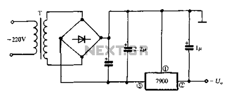
Negative voltage regulators, such as the LM79xx series, follow a topology distinct from their positive counterparts. The fundamental circuit consists of three terminals: input (VIN), ground (GND), and output (VOUT), where the output voltage is regulated to a negative value relative to ground. The input must be more negative than the output to maintain regulation.
Core Components
The minimal configuration requires:
- Input capacitor (CIN): Typically 0.33–1 µF, placed close to the regulator to suppress high-frequency noise and stabilize input impedance.
- Output capacitor (COUT): Usually 0.1–10 µF, ensuring stability under transient loads and reducing output ripple.
- Protection diodes: Optional but recommended to prevent reverse current flow during startup/shutdown.
Mathematical Analysis
The dropout voltage (VDO) for a negative regulator is defined as:
where VIN and VOUT are negative. For stable operation, VIN must satisfy:
The power dissipation (PD) is calculated as:
Practical Implementation
A typical LM7905 circuit (-5V output) with a -9V input includes:
- CIN = 0.33 µF (tantalum or ceramic) at the input.
- COUT = 0.1 µF at the output.
- 1N4001 diode across input-output to handle reverse transients.
Stability Considerations
Negative regulators exhibit higher sensitivity to capacitive load ESR. For stability:
where fc is the regulator's crossover frequency (typically 0.5–1 MHz for monolithic designs). Low-ESR ceramic capacitors may require a small series resistor (0.1–1 Ω) to avoid oscillation.
3.2 Input and Output Capacitor Selection
Stability and Transient Response Considerations
The selection of input and output capacitors in a negative voltage regulator circuit is critical for ensuring stability, minimizing output ripple, and improving transient response. Unlike positive regulators, negative regulators often exhibit different stability characteristics due to the inversion of feedback polarity. The output capacitor (COUT) must compensate for the regulator's internal pole while maintaining phase margin.
The minimum output capacitance required to ensure stability can be derived from the regulator's open-loop gain and phase response. For a typical negative linear regulator (e.g., LM337), the output capacitance must satisfy:
where fUGF is the unity-gain frequency of the regulator's error amplifier, and RESR is the equivalent series resistance of the capacitor. Excessive RESR can introduce a zero that degrades phase margin, while insufficient capacitance leads to poor load transient response.
Input Capacitor Requirements
The input capacitor (CIN) serves two primary purposes: reducing input voltage ripple and providing instantaneous current during load transients. For a negative regulator, the input capacitor must handle the reverse current flow during switching or transient conditions. The minimum input capacitance is determined by:
where IPEAK is the peak current demand, Δt is the transient duration, and ΔVIN is the allowable input voltage droop. Low-ESR ceramic capacitors (X5R/X7R) are preferred for high-frequency decoupling, while bulk electrolytic or tantalum capacitors handle slower transients.
Output Ripple and Noise Suppression
Output ripple voltage (VRIPPLE) is a function of the capacitor's impedance at the switching frequency. For a negative regulator, the ripple can be approximated by:
where fSW is the ripple frequency (or switching frequency in LDOs with bypass switching). Parallel combinations of ceramic and tantalum capacitors are often used to achieve low RESR and high capacitance density.
Practical Design Guidelines
- Stability: Ensure the output capacitor's RESR is within the regulator's specified range (typically 0.1Ω to 5Ω for most linear regulators).
- Transient Response: Use a combination of bulk and high-frequency capacitors to cover a wide bandwidth.
- Placement: Position CIN and COUT as close as possible to the regulator pins to minimize parasitic inductance.
In high-noise environments, additional filtering with an RC network at the output may be necessary to suppress high-frequency artifacts. The time constant of this network should not interfere with the regulator's control loop bandwidth.
3.3 Heat Dissipation and Thermal Considerations
Negative voltage regulators, like their positive counterparts, dissipate power as heat when operating under load. The power dissipation Pdiss is primarily governed by the voltage drop across the regulator and the output current. For a negative regulator with an input voltage Vin and output voltage Vout, the power dissipated is:
where Iload is the load current and Iq is the quiescent current of the regulator. The first term dominates in most practical applications, making thermal management critical for high-current or high-dropout scenarios.
Thermal Resistance and Junction Temperature
The junction temperature Tj of the regulator must be kept within safe limits to prevent thermal shutdown or degradation. The relationship between power dissipation, thermal resistance, and ambient temperature is:
where:
- Ta is the ambient temperature,
- θjc is the junction-to-case thermal resistance,
- θcs is the case-to-sink thermal resistance (if a heatsink is used),
- θsa is the sink-to-ambient thermal resistance.
For TO-220 packages, typical θjc values range from 1–5°C/W, while θja (junction-to-ambient without a heatsink) can exceed 50°C/W. Exceeding the maximum junction temperature (often 125–150°C) risks device failure.
Heatsink Selection and Design
Heatsinks reduce θsa to maintain Tj within limits. The required thermal resistance of the heatsink is derived by rearranging the junction temperature equation:
Forced air cooling can further reduce θsa by 30–50%. Thermal interface materials (TIMs) like silicone pads or thermal grease minimize θcs, typically achieving 0.1–1.0°C/W.
Practical Considerations
- PCB Layout: Copper pours or dedicated thermal vias improve heat dissipation in surface-mount designs.
- Transient Loads: Intermittent high-current loads may require thermal mass analysis to avoid peak Tj violations.
- Derating Curves: Manufacturers provide derating guidelines for elevated ambient temperatures.
3.4 Protection Mechanisms (Overcurrent, Overvoltage)
Overcurrent Protection
Negative voltage regulators, like their positive counterparts, must incorporate overcurrent protection to prevent catastrophic failure under excessive load conditions. The most common method employs a current-sensing resistor in series with the output, feeding a comparator that triggers a shutdown or current-limiting mechanism when the threshold is exceeded. For a regulator with a maximum output current Imax, the power dissipation in the pass transistor during a short-circuit event is given by:
where Vin is the input voltage and Vout is the regulated output voltage. Foldback current limiting is often implemented in high-power designs to reduce Pdiss under fault conditions, where the current limit decreases as Vout approaches zero.
Overvoltage Protection
Overvoltage events can occur due to input transients, inductive load kickback, or regulator failure. A crowbar circuit, typically using an SCR or zener-triggered MOSFET, is employed to clamp the output voltage to a safe level. The triggering voltage Vtrigger is set slightly above the nominal output:
where ΔVmargin accounts for normal regulation tolerances. For negative regulators, the protection circuitry must account for the inverted polarity, often requiring P-channel devices or careful level-shifting of control signals.
Thermal Considerations
Protection circuits must account for thermal runaway in bipolar designs, where increased junction temperature raises leakage currents, further increasing dissipation. Modern IC regulators integrate temperature sensors that enforce a derating curve:
with Tj as junction temperature and Tamb as ambient temperature. This necessitates careful PCB layout to ensure accurate thermal sensing.
Practical Implementation
In the LM337 adjustable negative regulator, the internal protection network includes:
- Darlington pass transistor with current limiting at ≈ 2.2A
- Thermal shutdown at 150°C (typical)
- Safe operating area (SOA) protection through dynamic current limiting
For mission-critical applications, external TVS diodes (e.g., SMAJ series) provide additional transient suppression, with breakdown voltages selected per:
where the 30% margin accounts for temperature coefficients and aging effects.
4. Use in Audio Amplifiers
4.1 Use in Audio Amplifiers
Negative voltage regulators play a critical role in audio amplifier designs, particularly in dual-rail power supplies that require symmetric positive and negative voltage rails. High-fidelity audio circuits, such as operational amplifier (op-amp) stages and Class-AB amplifiers, depend on stable negative voltage rails to minimize distortion and ensure proper biasing of complementary output transistors.
Biasing and Signal Integrity
In Class-AB amplifiers, the output stage consists of complementary NPN and PNP transistors. A negative voltage regulator (e.g., LM337 or 79xx series) ensures the PNP transistor operates in its active region without crossover distortion. The regulator maintains a constant negative rail voltage, preventing thermal drift and load-induced fluctuations that degrade Total Harmonic Distortion (THD) performance.
Where Vref is the reference voltage (typically -1.25V for LM337), R1 and R2 set the output voltage, and Iadj is the adjustment pin current (≈50µA).
Noise Suppression Techniques
Audio amplifiers are sensitive to power supply noise, which manifests as audible hum or hiss. Negative regulators mitigate this by:
- Low Dropout (LDO) Designs: Minimizing input-output differentials reduces thermal noise.
- Decoupling Networks: Pairing the regulator with low-ESR capacitors (e.g., 10µF tantalum + 0.1µF ceramic) suppresses high-frequency ripple.
- Ground Plane Isolation: Separating analog and digital grounds prevents ground loops.
Case Study: Op-amp Rail Splitting
In a ±15V op-amp supply, a 7915 negative regulator paired with a 7815 positive regulator creates a balanced dual-rail system. Asymmetry in rail voltages introduces DC offset, distorting the output waveform. The regulator’s line regulation (typically 0.01%/V) ensures symmetry even with varying input voltages.
Thermal Considerations
Negative regulators dissipate power as:
In high-current audio stages (e.g., >500mA), heat sinks or switching preregulators (e.g., Buck-Boost converters) are necessary to maintain junction temperatures below 125°C for reliable operation.
4.2 Role in Bipolar Power Supplies
Negative voltage regulators are essential in bipolar power supplies, where symmetrical positive and negative rails are required. These regulators maintain a stable negative output voltage despite variations in input voltage or load conditions, ensuring balanced operation in analog circuits such as operational amplifiers, data converters, and audio systems.
Symmetrical Voltage Regulation
In bipolar supplies, the negative regulator complements the positive regulator to achieve dual-rail operation. The relationship between input and output voltages is governed by:
where Vref is the reference voltage (typically -1.25 V for LM337), R1 and R2 are feedback resistors, and Iadj is the adjustment pin current. The negative regulator mirrors the positive regulator's behavior but inverts the output polarity.
Stability Considerations
Bipolar supplies demand matched transient response and load regulation between positive and negative regulators. Key stability factors include:
- Output impedance matching: Mismatches cause ground bounce and signal distortion.
- Decoupling network symmetry: Identical capacitor values (e.g., 10 µF tantalum + 100 nF ceramic) must be used on both rails.
- Thermal coupling: Co-locating regulators on the same heatsink minimizes temperature-induced drift.
Practical Implementation
A typical bipolar supply using LM317 (positive) and LM337 (negative) requires:
The ground reference becomes critical in such configurations. Any impedance in the ground path introduces errors, necessitating a star grounding topology for precision applications.
Noise and Ripple Rejection
Negative regulators exhibit comparable PSRR (Power Supply Rejection Ratio) to their positive counterparts. For the LM337:
However, in bipolar configurations, differential noise becomes a concern. Cross-coupling through shared ground paths can degrade system performance, requiring:
- Separate feedback networks for each regulator
- Low-ESR capacitors at both input and output
- Guard rings around sensitive analog sections
Current Balancing
Asymmetric loading between rails causes DC offset errors. The current imbalance ΔI relates to offset voltage Vos through:
where Zgnd is ground impedance and Zreg is regulator output impedance. Active current balancing techniques using sense resistors and error amplifiers may be employed in critical applications.
4.3 Industrial and Laboratory Equipment
Stability Requirements in Precision Systems
Negative voltage regulators in industrial and laboratory settings must maintain ultra-low output noise and high power supply rejection ratio (PSRR) to avoid interference with sensitive analog instrumentation. For instance, operational amplifiers and data acquisition systems often require bipolar supplies (±15V or ±5V) with ripple rejection exceeding 80 dB at 100 Hz. The relationship between PSRR and output noise can be modeled as:
where f is the noise frequency, and ΔVin/ΔVout represents the input-to-output noise attenuation.
Thermal Management in High-Current Applications
Industrial loads such as motor controllers or RF amplifiers demand regulators like the LM337 with current handling beyond 1.5A. The junction-to-ambient thermal resistance (θJA) must be minimized to prevent thermal shutdown. For a TO-220 package dissipating 10W:
where Tj is junction temperature, Ta is ambient temperature, and Pd is power dissipation. Active cooling or heatsinks are often mandatory for θJA values below 40°C/W.
Case Study: Mass Spectrometer Power Supply
A -1250V bias supply for ion detectors exemplifies custom regulator designs. Here, a Zener-referenced pass transistor (e.g., 2N6515) with optocoupled feedback ensures stability. Key parameters include:
- Load regulation: <0.01%/mA
- Temperature coefficient: ±50 ppm/°C
- Output capacitance: <1 pF to avoid parasitic oscillations
Fault Protection Mechanisms
Industrial regulators integrate foldback current limiting and safe operating area (SOA) protection. For a -12V/3A supply, the SOA boundary is defined by:
where VDS is drain-source voltage and ID is drain current. This prevents catastrophic failure during load transients.
EMI Compliance Challenges
Switching negative regulators (e.g., LTspice-simulated buck-boost topologies) must suppress conducted emissions below CISPR 22 Class B limits. A π-filter with X7R ceramics achieves >40 dB attenuation at 1 MHz:
5. Output Voltage Instability
5.1 Output Voltage Instability
Output voltage instability in negative voltage regulators arises from multiple factors, including load transients, thermal drift, and feedback loop dynamics. Unlike positive regulators, negative regulators must handle inverted control signals, which can introduce phase shifts and exacerbate instability.
Feedback Loop Stability
The stability of a negative voltage regulator is governed by its feedback loop, where the error amplifier compares a fraction of the output voltage to a reference. The loop gain L(s) is given by:
where AOL(s) is the open-loop gain of the error amplifier and β(s) is the feedback factor. For stability, the phase margin must exceed 45° at the crossover frequency where |L(s)| = 1.
Thermal and Load Effects
Thermal gradients across the regulator IC can induce voltage drift due to temperature-dependent variations in the bandgap reference and pass transistor characteristics. Load transients, particularly in switching regulators, cause abrupt changes in output current, leading to undershoot or overshoot if the control loop cannot respond quickly enough.
where ΔIload is the load step, Cout is the output capacitance, and tresponse is the regulator's settling time.
Compensation Techniques
To mitigate instability, compensation networks are employed. A dominant pole at the error amplifier output ensures high DC gain while rolling off at higher frequencies. A zero is introduced to counteract phase lag:
where Rcomp and Ccomp are the compensation components, and Resr is the equivalent series resistance of the output capacitor.
Practical Considerations
- PCB Layout: Ground loops and parasitic inductances can degrade stability. A star ground topology minimizes noise coupling.
- Component Selection: Low-Resr capacitors (e.g., ceramic) reduce output ripple but may require additional ESR compensation.
- Simulation: SPICE models of the regulator and load should be validated for transient response and phase margin.
Case Study: LM337 Instability
The LM337, a common adjustable negative regulator, exhibits oscillation when the output capacitance exceeds 10µF without proper ESR. The datasheet mandates a minimum ESR of 0.1Ω–0.5Ω to ensure stability. This constraint arises from the non-inverting feedback architecture, which is more sensitive to capacitive loads than positive regulators.
5.2 Excessive Heat Generation
Negative voltage regulators, like their positive counterparts, dissipate power as heat when regulating higher input voltages to lower output levels. The primary mechanism of heat generation stems from the voltage drop across the pass transistor and the associated current flow. The power dissipation Pdiss is given by:
where Vin is the input voltage, Vout the regulated output voltage, Iload the load current, and Iq the quiescent current of the regulator itself. The first term represents the dominant power loss due to the voltage differential, while the second accounts for internal circuit inefficiencies.
Thermal Resistance and Junction Temperature
The regulator's ability to dissipate heat is constrained by its thermal resistance θJA (junction-to-ambient). The junction temperature TJ is calculated as:
where TA is the ambient temperature. Exceeding the maximum junction temperature (typically 125–150°C for silicon devices) triggers thermal shutdown or irreversible damage. For example, an LM337 with θJA = 50°C/W dissipating 5W in a 25°C ambient reaches:
This far exceeds safe limits, necessitating heat sinks or improved thermal management.
Mitigation Strategies
- Heat Sinking: Attaching a heat sink reduces effective θJA by lowering the thermal resistance path. The total resistance becomes:
where θJC (junction-to-case), θCS (case-to-sink), and θSA (sink-to-ambient) are additive.
- Switching Regulators: For high differential voltages, switching topologies (e.g., buck converters) minimize dissipation by storing energy inductively rather than burning it as heat.
- Parallel Regulation: Distributing the load across multiple regulators reduces individual power dissipation.
Real-World Implications
In aerospace applications, where ambient temperatures vary drastically, designers must account for worst-case TA and derate components accordingly. For instance, a -15V regulator powering an RF amplifier in a satellite must ensure TJ remains within bounds even during solar heating phases.
5.3 Noise and Ripple Problems
Sources of Noise in Negative Voltage Regulators
Negative voltage regulators, like their positive counterparts, are susceptible to noise and ripple originating from both internal and external sources. Internally, thermal noise in the pass transistor, shot noise from current flow across semiconductor junctions, and flicker noise (1/f noise) in the error amplifier contribute to output voltage fluctuations. Externally, conducted noise from the input supply and radiated electromagnetic interference (EMI) can couple into the regulator's feedback network.
where k is Boltzmann's constant, T is temperature in Kelvin, R is the resistance, and Δf is the bandwidth.
Ripple Rejection and Power Supply Rejection Ratio (PSRR)
The ability of a regulator to attenuate input ripple is quantified by its Power Supply Rejection Ratio (PSRR), defined as:
For negative regulators such as the LM337, PSRR typically exceeds 60 dB at low frequencies (below 100 Hz) but degrades at higher frequencies due to the limited bandwidth of the internal error amplifier. The PSRR roll-off follows a first-order response:
where fc is the corner frequency (typically 1-10 kHz for linear regulators).
Minimizing Output Ripple
Three primary methods exist for reducing output ripple in negative voltage regulator circuits:
- Input Filtering: A low-ESR ceramic capacitor (0.1-1 μF) placed directly at the input pin shunts high-frequency noise to ground. For switching converters feeding the regulator, an additional LC filter with a cutoff frequency below the switching frequency is critical.
- Output Filtering: While negative regulators require a minimum load capacitance for stability (often specified in datasheets), adding a parallel combination of a low-ESR tantalum capacitor (10 μF) and a ceramic capacitor (0.1 μF) improves high-frequency rejection.
- Ground Plane Management: Since negative regulators reference the output voltage rather than ground, improper grounding can create ground loops that inject noise. A star grounding scheme, where all filter capacitors and load returns connect at a single point near the regulator's ground pin, minimizes this effect.
Case Study: Noise in Adjustable Negative Regulators
Adjustable negative regulators like the LM337 introduce additional noise through the feedback resistor network. The noise gain of the circuit amplifies the regulator's internal noise by:
where R1 and R2 set the output voltage. Bypassing R2 with a capacitor (C_{adj) creates a low-pass filter for the feedback path, reducing high-frequency noise. The optimal value balances stability and noise rejection:
where fc should be at least one decade below the regulator's unity-gain bandwidth.
6. Recommended Datasheets and Manuals
6.1 Recommended Datasheets and Manuals
- PDF Voltage Regulators Selection Guide - electricalmanuals.net — Voltage Regulators Selection Guide TABLE 2 Typical Regulator Designs, 50 Hz Item Voltage Current kVA ±10%* ±8.75%* ±7.5%* ±6.25%* ±5%* BIL Mounting Future ONAF Connectors Low Rating or Clamp Live ONAF Part (mm) 1 6600 50 33 50 55 60 68 80 95 Pole/Platform N/A #6 - 250 1716 2 6600 100 66 100 110 120 135 160 95 Pole/Platform N/A #6 - 250 1818
- PDF TPS7A33 36-V, 1-A, Ultralow-Noise Negative Voltage Regulator datasheet ... — TPS7A33 -36-V, 1-A, Ultralow-Noise Negative Voltage Regulator 1 Features 3 Description The TPS7A33 series of linear regulators are negative 1• Input Voltage Range: -3 V to -36 V voltage (-36 V), ultralow-noise (16-μVRMS, 72-dB • Noise: PSRR) linear regulators capable of sourcing a - 16 μVRMS (10 Hz to 100 kHz) maximum load of 1 A.
- PDF Datasheet - RHFL7913A - Rad-hard adjustable negative voltage regulator — The RHFL7913A adjustable is a high performance Rad hard negative voltage regulator. Available in FLAT-16 and new SMD5C hermetic ceramic packages, it is specifically intended for space and harsh radiation environments. It provides exceptional electrical performances, high speed and low dropout voltage. Input supply ranges from - 3 V to - 12 V.
- PDF Negative Voltage Regulators - onsemi — CURRENT NEGATIVE FIXED VOLTAGE REGULATORS TO−92 P SUFFIX CASE 29−10 SOIC−8 D SUFFIX CASE 751 MARKING DIAGRAMS See detailed ordering and shipping information in the package dimensions section on page 7 of this data sheet. ORDERING INFORMATION Pin 1. Ground 2. Input 3. Output Pin 1. Vout 2. Vin 3. Vin 4. NC 5. GND 6. Vin 7. Vin 8. NC xxx ...
- PDF LM2991 Negative Low-Dropout Adjustable Regulator datasheet (Rev. I) — An IMPORTANT NOTICE at the end of this data sheet addresses availability, warranty, changes, use in safety-critical applications, intellectual property matters and other important disclaimers. PRODUCTION DATA. LM2991 SNVS099I -MAY 1999-REVISED OCTOBER 2016 LM2991 Negative Low-Dropout Adjustable Regulator 1 1 Features
- PDF LM337-N 3-Terminal Adjustable Negative Regulators datasheet — • IGBT Drive Negative Gate Supplies • Networking • Set-Top Boxes 3 Description The LM337-N-MIL is an adjustable 3-terminal negative voltage regulator capable of supplying −1.5 A or more currents over an output voltage range of −1.25 V to −37 V. It requires only two external resistors to set the output voltage and one output
- PDF Negative Voltage Regulators - onsemi — These negative regulators are available in the same seven−voltage options as the MC7800 devices. In addition, one extra voltage option commonly employed in MECL systems is also available in the negative MC7900 series. Available in fixed output voltage options from −5.0 V to −24 V, these regulators employ current limiting, thermal shutdown ...
- PDF TPS723 200-mA, Low-Noise, High-PSRR, Negative Output Low-Dropout Linear ... — The TPS723 low-dropout (LDO) negative voltage regulator offers an ideal combination of features to support low noise applications. This device is capable of operating with input voltages from -10 V to -2.7 V, and support outputs from -10 V to -1.2 V. This regulator is stable with small, low-cost ceramic capacitors, and include enable ...
- PDF CL-7 voltage regulator control and accessories catalog — 2 Catalog Data CA225003EN Effective August 2024 CL-7 microprocessor-based voltage regulator control and accessories EATON www.eaton.com Ordering information When ordering a voltage regulator with a CL-7 voltage regulator control, construct the control catalog number using Table 1. Select the appropriate digits of the catalog number based upon control feature requirements.
- PDF Voltage regulator communication-ready controls specification (PDF) — automatic/remote or manual/local operation of the voltage regulator. Monitoring of the control is available at all positions. 3.2.1.3. A momentary three-position RAISE-OFF-LOWER control switch, which shall be active only when the adjacent control switch is in the MANUAL position. The switch must be
6.2 Advanced Topics and Research Papers
- (Pdf) Design and Construction of A Dual Regulated ±0-35volts Dc Power ... — For LPF, (26) (27) 2.5 VOLTAGE REGULATORS CIRCUIT In this work, two voltage regulators LM317 (positive voltage) and LM337 (negative voltage) were used to obtained a dual polarity (±) of DC output. 2.5.1 LM317 (Positive Voltage Regulator) The LM317 is a three terminal positive voltage regulator with an adjustable output voltage capable of ...
- (PDF) Advanced Practical Electronics - Circuits & Systems - ResearchGate — Advanced Practical Electronics - Circuits & Systems. August 2021; ... 2.4.1 Linear Voltage Regulators ... 6.2.6.2 Linear Variable Differential Transformers ...
- OP-AMP Applications, Timer, Voltage Regulator, and Converter — 6.9.1.2 Fixed Negative Voltage Regulator. The series 7900 ICs provide negative regulation, similarly to those providing positive voltages. 6.9.2 Adjustable Voltage Regulator. Voltage regulators are also provided in circuit configuration that allows the users to set the output voltage regulated value.
- LM137, LM337-N 3-Terminal Adjustable Negative Regulators — LM137, LM337-N www.ti.com SNVS778E -MAY 1999-REVISED JANUARY 2016 6.5 Electrical Characteristics Unless otherwise specified, these specifications apply −55°C ≤Tj ≤150°C for the LM137, 0°C ≤Tj ≤125°C for the LM337-N; VIN −VOUT = 5 V; and IOUT = 0.1 A for the TO package and IOUT = 0.5 A for the SOT-223 and TO-220 packages. Although power dissipation is internally limited ...
- Voltage Regulator - an overview | ScienceDirect Topics — The automatic voltage regulator is a device that is changing the output voltage to keep the critical load voltage at a sufficient level, and it does it by changing the transformer tap or other methods, mechanically or electronically [122]. ... Basic two-transistor negative regulator. This circuit is popular because of its extreme cheapness, but ...
- A Negative Low-Voltage Power Supply Integrated With High-Voltage ... — A negative low-voltage power supply with the highest positive potential as reference is proposed in this paper. The proposed power supply is integrated with high-voltage devices. When the high-voltage devices are applied as a switch, negative low-voltage pulses are first produced from the positive high voltage applied on devices by using the designed junction termination of the devices. Then ...
- A comprehensive review of improving power quality using active power ... — The topology was addressed as the line voltage regulator/condition. H. Fujita, and H. Akagi named the configuration as the unified power quality conditioner (UPQC) and verified the viability and effectiveness of the UPQC based on the experimental results of a laboratory 20 kV system [67, 68].
- PDF Effective Voltage Regulator For Domestic Loads - ijrar.org — The voltage regulator requires less cost as we are using serial voltage compensation instead of power electronic devices and the efficiency increases even the size of the equipment is reduced. In this paper we were discussing about single phase voltage regulator it could be extended for three phase networks.
- (PDF) Development of an Automatic Voltage Regulator with a Good ... — It is observed that the automatic voltage regulator managed to achieve up to 2% voltage regulation at full load operation of 500 W. A thyristor controller is used to control the excitation voltage.
- Analysis and Design of Voltage Controlled Current Source for LDO ... — A low dropout (LDO) voltage regulator with high power supply rejection ratio (PSRR) and low temperature coefficient (TC) is presented in this paper. Large 1µF off-chip load capacitor is used to achieve the high PSRR.
6.3 Online Resources and Communities
- LM137, LM337-N 3-Terminal Adjustable Negative Regulators — LM137, LM337-N www.ti.com SNVS778E -MAY 1999-REVISED JANUARY 2016 6.5 Electrical Characteristics Unless otherwise specified, these specifications apply −55°C ≤Tj ≤150°C for the LM137, 0°C ≤Tj ≤125°C for the LM337-N; VIN −VOUT = 5 V; and IOUT = 0.1 A for the TO package and IOUT = 0.5 A for the SOT-223 and TO-220 packages. Although power dissipation is internally limited ...
- PDF LM337-N 3-Terminal Adjustable Negative Regulators — • IGBT Drive Negative Gate Supplies • Networking • Set-Top Boxes 3 Description The LM337-N-MIL is an adjustable 3-terminal negative voltage regulator capable of supplying −1.5 A or more currents over an output voltage range of −1.25 V to −37 V. It requires only two external resistors to set the output voltage and one output
- PDF LM137QML 3-Terminal Adjustable Negative Regulators — The LM137 are adjustable 3-terminal negative voltage regulators capable ofsupplying in excess 1.5 A over an output voltage range of −37 V to −1.2 V. These regulators are exceptionally easy to apply, requiring only 2 external resistors to set the output voltage and 1 output capacitor for frequency compensation. The circuit design has been ...
- 6.3 V LDO Voltage Regulators - Mouser - Mouser Electronics — LDO Voltage Regulators 28V Low Power Consumption 150mA Voltage Regulators (with Stand-by Function) AEC-Q100 Grade2 qualified XD6216B631MR-G Torex Semiconductor
- 6.3v Regulator? - Page 1 - EEVblog — Tube shortwave Rx here has regulated plate and heater supplies for the RF section ( 2 of 6BE6, 1 of 6BA6 and 1 of 6AV6) The plate is by a pwm booster. Heater Regulator: Heaters are regulated by a 7805, TO220 , standing on resistors to give 6.12 V R_upper = 270 Ohm, R_lower = 56 Ohm The (4) tubes + pilot lamp draw 1.04 Amp DC. The receiver has run like that, DDS locked almost continuously for 2 ...
- PDF NEGATIVE VOLTAGE REGULATORS - Farnell — The L7900 series of three-terminal negative regulators is available in TO-220, TO-220FP, TO-3 and D2PAK packages and several fixed output voltages, making it useful in a wide range of ... NEGATIVE VOLTAGE REGULATORS Figure 1: Schematic Diagram TO-220 D2PAK TO-220FP TO-3 Rev. 10. L7900 SERIES 2/18
- 6.3V Voltage Regulators - Linear, Low Drop Out (LDO) Regulators — 6.3V Integrated Circuits (ICs) - Voltage Regulators - Linear, Low Drop Out (LDO) Regulators are in stock at Digikey. Order Now! 6.3V Integrated Circuits (ICs) ship same day
- Voltage Regulators II - sound-au.com — 1 - Reference Voltage. In any regulator (voltage or current), a stable reference voltage is required. It doesn't matter if the output is a fixed or variable voltage, a reference is still necessary. For most simple supplies, a zener diode is the easiest and cheapest, but it is not the most accurate.
- Negative voltage regulators - Electrical Engineering Stack Exchange — Simple answer: You would get 5V in your case, but referenced to -12V instead of ground. In other words, you would have -7V, not -5V. In addition, the regulator would only source current onto the -7V rail, not sink it as would be expected for a negative voltage.. If you want to run some circuitry from 5V between -7V and -12V (the -12V will be the ground for this circuitry), then you can use a ...