
No inductive analog relay circuit
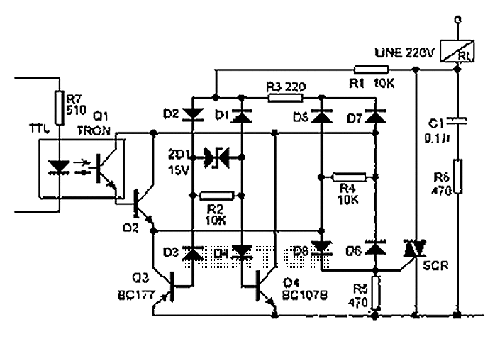
The circuit operates on a 220V AC power supply, which is connected to an inductive load (RL) and various components that help manage the switching and protection of the system. The resistors R1 and R3 are used to limit the current and provide necessary biasing for the transistors Q3 and Q4, which are configured to alternate their conduction states. This alternation creates positive and negative half-cycle offsets, crucial for the operation of the subsequent components.
Diodes D1 to D4 function as rectifiers, converting the AC input into a usable form for the relay operation. The zener diode ZD1 is included to clamp the voltage and protect the circuit from overvoltage conditions. The optocouplers, represented by Q1, are essential for isolating the control signal from the high-voltage side of the circuit. They enable safe interfacing between the low-voltage TTL logic and the high-voltage components without risking damage.
When the TTL circuit outputs a high signal, the optocouplers conduct during the positive half-cycle, resulting in a voltage drop across resistor R5. This drop is sufficient to trigger the SCR, allowing current to flow through the load RL, thus activating it. The design ensures that there is no reverse induced voltage generated, which is a common issue in inductive loads that can lead to component failure.
Capacitor C1 and resistor R6 are crucial for absorbing voltage spikes and smoothing the current flow, further protecting the circuit from potential damage caused by inductive kickback. The limitation provided by R3 is vital to ensure that the circuit remains stable and operates within safe parameters, especially when dealing with inductive loads that can create significant phase shifts in the voltage supply.
In summary, this circuit design effectively utilizes transistors, diodes, and optocouplers to create a robust relay system that operates safely and efficiently while minimizing risks associated with inductive loads and high-voltage operations. As shown in FIG relay is non-inductive analog circuit theory. working principle: 220V power supply via a load RL, R1, D1 ~ D4, ZD1, as Q4, Q3 in turn provide positive and negat ive half cycle offset; through R3, D5 ~ D8 provides power for the optocouplers Q1 simultaneously. When the current level TTL circuit outputs a high level signal, optocouplers in the city turned positive half-cycle, thus producing a pressure drop R5 ends, triggering SCR conduction, electrical work load RL. As a function of the entire circuit relay, but will not produce the reverse induced voltage, thus avoiding the load is high back pressure breakdown the possibility of damage.
C1, R6 pulse absorbing element, R3 from limiting the role. To avoid RL when inductive load, 90 phase thyristor power supply voltage generated by optocouplers, power optocouplers this circuit is taken from the SCR anode instead of directly from the mains.
Related Circuits
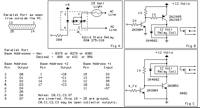
Below are three examples of controlling a relay from the PC's parallel printer port (LPT1 or LPT2). Figure A shows a solid-state relay controlled by one of the parallel port data lines (D0-D7) using a 300-ohm resistor and a...
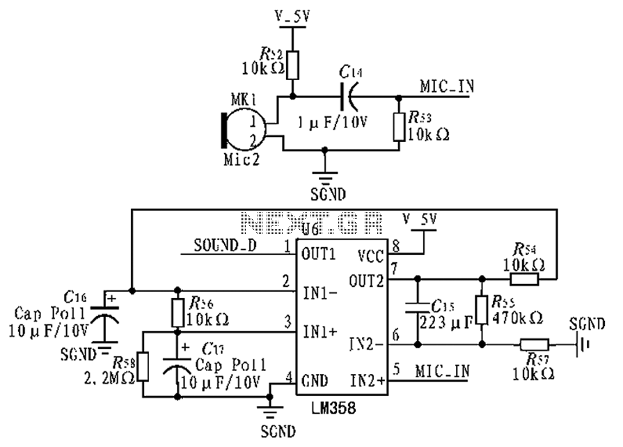
The circuit diagram focuses on the research and design features applied to mobile robots. The design considers small size, low power consumption, and ease of movement, catering to home users with a user-friendly display interface. For speech recognition, a...
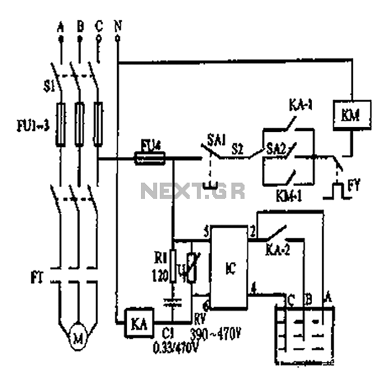
An automatic water tank system is illustrated in the circuit diagram. The circuit employs a PSSR AC solid-state relay, which is a new type of solid-state relay designed for AC applications. Unlike traditional solid-state relays (SSR), this PSSR not...
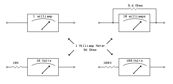
A milliamp meter can be utilized as a voltmeter by incorporating a series resistance. The required resistance is calculated by dividing the full-scale voltage reading by the full-scale current of the meter movement. For example, using a 1 milliamp...
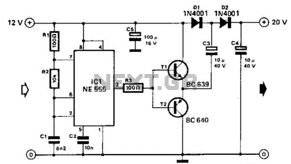
Using a 555 timer and voltage doubler, this circuit will supply over 50 mA at 20 V DC. Transistors T1 and T2 act as power amplifiers to drive the voltage doubler. The frequency of operation is approximately 8.5 kHz. The...
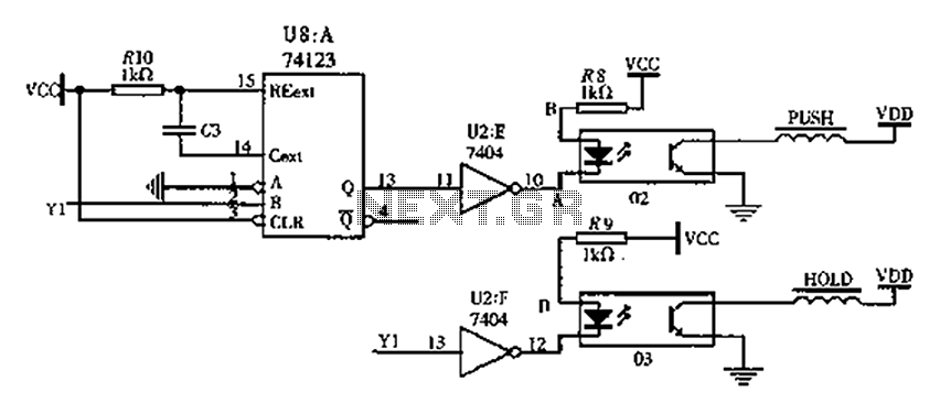
The FIG switching solenoid driver circuit utilizes the 74123 device chip (U8) and solid-state relays (02, 03). The switching electromagnet coil is referred to as the PUSH coil, while the HOL is maintained at a power supply voltage (VDD)...