On-off-inverters

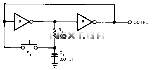
Each time the switch is closed, the voltage across capacitor C1 causes inverter A to change state, with positive feedback from inverter B. Resistor R1 delays the charging and discharging of C1, rendering the circuit nearly immune to contact bounce. This circuit operates effectively with both CMOS and TTL gates. The values of R1 and C1 are not critical and can be increased for enhanced protection against contact bounce, if necessary. Recommended ranges are 10 kΩ to 1 MΩ for R1, and 0.01 µF to 1.0 µF for C1.
The circuit described operates as a debounce circuit utilizing two inverters configured in a feedback loop. When the switch is activated, it generates a momentary change in voltage that is detected by capacitor C1. The initial change in voltage causes inverter A to switch states. This transition is reinforced by the positive feedback provided by inverter B, ensuring that once the state change occurs, it is maintained until the switch is released.
Resistor R1 plays a critical role in the timing characteristics of the circuit. It limits the rate at which capacitor C1 charges and discharges, effectively filtering out any rapid fluctuations in voltage that could occur due to mechanical bouncing of the switch contacts. This characteristic is crucial for applications where reliable switching is necessary, as it prevents false triggering caused by transient signals.
The choice of values for R1 and C1 can be adjusted based on the specific requirements of the application. While the circuit can function with a wide range of resistor and capacitor values, it is advisable to select components that provide adequate debounce time without introducing excessive delay. The recommended resistor values between 10 kΩ and 1 MΩ and capacitor values between 0.01 µF and 1.0 µF allow for flexibility in tuning the circuit's response time.
This debounce circuit is versatile and can be employed in various electronic applications where switch bounce is a concern, making it suitable for both CMOS and TTL logic families. The simplicity of the design, combined with its effectiveness, makes it a valuable component in digital systems where reliable input signals are essential.Each time the switch closes, the voltage on Cl causes inverter A to change state, with positive feedback from inverter B. Resistor Rl delays the charging and discharging of Cl, making the circuit virtually immune to contact bounce.
The circuit works with either CMOS or TTL gates. The values of R1 and C1 are not critical and can be increased for greater contact bounce protection, if needed. Recommended ranges are 10 K to 1 MO for Rl, and 0.01 to 1.0 p.F for Cl.