
Operational-amplifiers
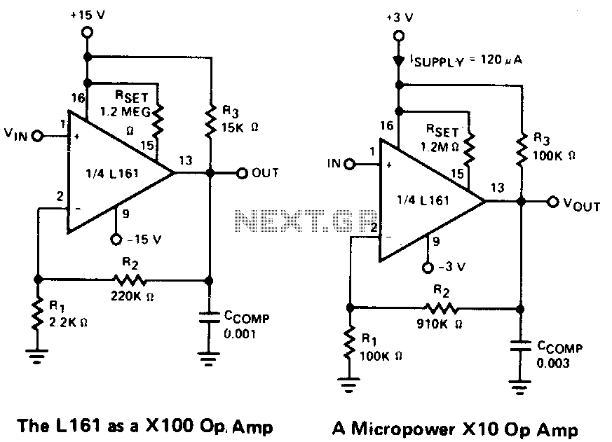
This is a single gain-of-100 amplifier with a gain-bandwidth product of 20 MHz. The primary limitation in performance is the low slew rate of 0.3 V/μs imposed by the charging of Ccomp. The effects of slew rate and compensation are discussed. A lower gain amplifier requires a larger Ccomp, which further reduces the slew rate. Therefore, in certain applications, it may be advantageous to decrease the gain by implementing a resistive divider at the input instead of increasing R1. Additionally, Figure 66-1B illustrates a 700 μW, x10 operational amplifier with a slew rate of 0.02 V/μs, which is 3 dB down at 100 kHz.
The described amplifier is a single-stage operational amplifier characterized by a fixed gain of 100 and a gain-bandwidth product of 20 MHz. This means that the amplifier can maintain its gain across a frequency range up to 200 kHz, as the gain-bandwidth product is constant. The performance limitation arises from the slew rate, which is defined as the maximum rate of change of the output voltage. With a slew rate of 0.3 V/μs, the amplifier can only respond to rapid changes in input signals up to a certain frequency before distortion occurs.
Compensation capacitors, denoted as Ccomp, play a crucial role in stabilizing the amplifier's performance, especially in high-frequency applications. However, increasing the size of Ccomp to enhance stability can lead to a further reduction in the slew rate, creating a trade-off between stability and speed. This characteristic suggests that for applications requiring faster response times, a lower gain configuration may be beneficial. By using a resistive divider at the input to reduce the effective gain, the amplifier can accommodate larger compensation capacitance without significantly impairing the slew rate.
The additional example provided, Figure 66-1B, refers to a different operational amplifier with a lower power output of 700 μW and a gain of 10. This amplifier exhibits a much lower slew rate of 0.02 V/μs and reaches a 3 dB drop-off at 100 kHz. This emphasizes the relationship between power consumption, gain, and frequency response in operational amplifier design, suggesting that lower power amplifiers may struggle with higher frequency signals, further illustrating the importance of careful selection of gain and compensation components in circuit design.This is a single gain-of-100 amplifier with a gain-bandwidth product of 20 MHz! The primary limitation in the performance is the low slew rate (0.3 VIJ1s) imposed by IoH charging CcoMP· The effects of slew rate and compensation are shown. A lower gain amplifier requires a larger CcoMP, which in turn further reduces slew rate. For this reason, it might actually be advantageous in certain areas to lower the gain by placing a resistive divider at the input rather than raising R1.
Figure 66-lB shows a 700-JlW, XlO op amp whose slew rate is 0. 02 VIJlS and is 3 dB down at 100 kHz. 🔗 External reference
Warning: include(partials/cookie-banner.php): Failed to open stream: Permission denied in /var/www/html/nextgr/view-circuit.php on line 713
Warning: include(): Failed opening 'partials/cookie-banner.php' for inclusion (include_path='.:/usr/share/php') in /var/www/html/nextgr/view-circuit.php on line 713