
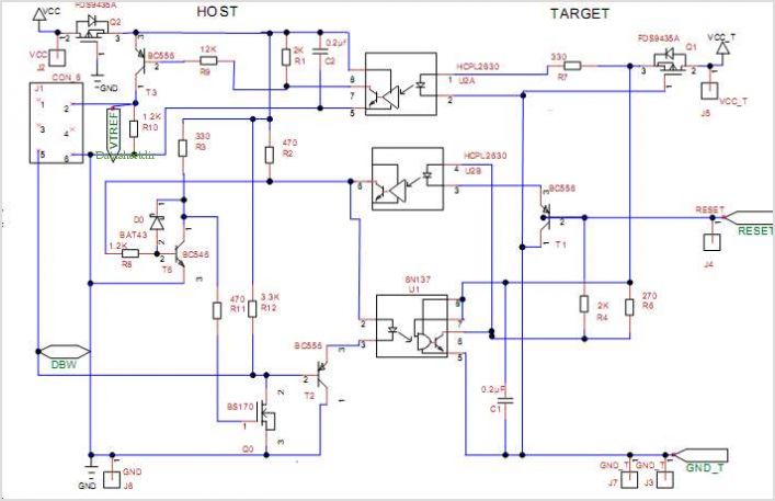
Opto Isolated Emulation For The Debugwire
The power circuit is essential for providing stable and reliable voltage levels to the various components of the UC3B device. It typically includes voltage regulators, capacitors for filtering, and protection diodes to prevent reverse polarity and overvoltage conditions. The reset circuit ensures that the device starts in a known state, utilizing a reset button or an external signal to initiate the reset process.
The USB connection facilitates communication and power supply between the UC3B device and external peripherals. It is crucial to ensure proper termination and impedance matching to maintain signal integrity. The ABDAC sound DAC interface allows for high-quality audio output, requiring careful consideration of the audio signal path and grounding to minimize noise.
JTAG and Nexus debug ports are critical for programming and debugging the device. These interfaces must be correctly configured to allow for seamless communication with development tools. Clocks and crystal oscillators are vital for timing and synchronization within the circuit. The selection of appropriate frequency and stability specifications is necessary to meet the operational requirements of the UC3B device.
When designing the schematic, it is important to follow a checklist that includes verifying pin assignments, ensuring proper grounding, confirming component values, and checking for signal integrity. This checklist serves as a guide to ensure that all essential aspects of the design are addressed, ultimately leading to a successful implementation of the UC3B device.Power circuit Reset circuit USB connection ABDAC sound DAC Interface JTAG and Nexus debug ports Clocks and crystal Oscillators 1 Introduction A good hardware design comes from a proper schematic. Since UC3B devices have a fair number of pins and functions, the schematic for these devices CAN be large and quite complex.
This application note d escribes a common checklist which should be used when starting and reviewing the schematics for a UC3B design. 🔗 External reference
Related Circuits
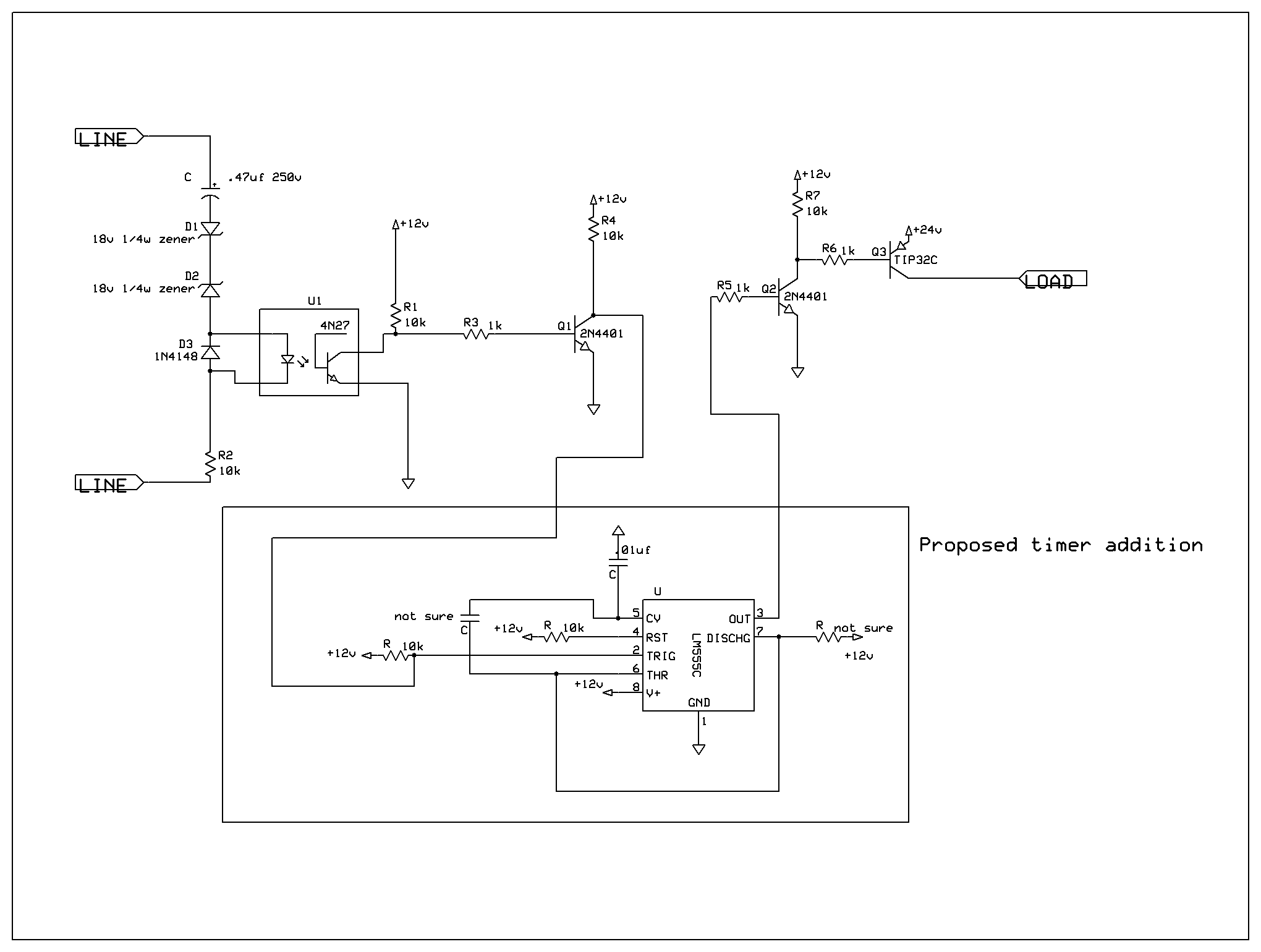
A ringer interface circuit is designed to buffer the output of a central telephone system, which connects to multiple ringers distributed throughout a building. This circuit addresses an issue where the line overloads when ringing, requiring a reset. The...
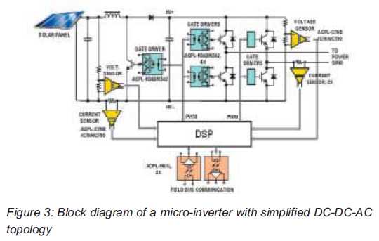
Both help improve efficiency and protect micro-inverters in photovoltaic (PV) solar applications. In 2009, the residential solar photovoltaic (PV) inverter market represented 90 percent of the total PV. The integration of micro-inverters in photovoltaic solar applications has significantly enhanced system...
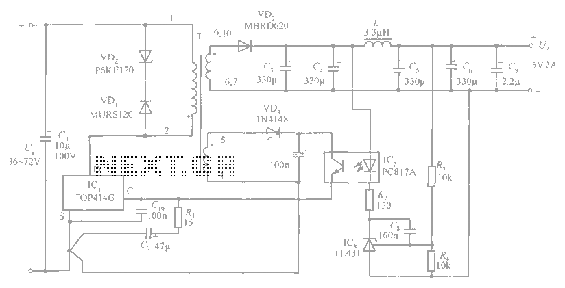
The circuit diagram includes an input filter capacitor C1 and a primary clamp composed of VDz and VD1. The resistor R1 is connected to the control terminal. C2 serves as a bypass capacitor. The TOP414GC-S is connected in parallel...
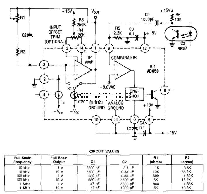
In this circuit, the input from the IC2 optocoupler is connected to the comparator input of the AD650 (Analog Devices or Maxim Electronics) voltage-to-frequency (V/F) converter. This converter internally generates a pulse that is sent to the operational amplifier,...

Miniature isolated AC/DC power supply. This circuit employs a novel method to generate a fully isolated and regulated 5 volts at 30 mA from the 120 VAC power line. It utilizes two tiny SCRs that operate alternately. The miniature isolated...
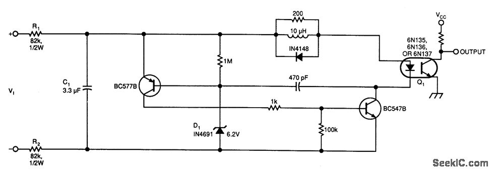
This circuit below illustrates a simple voltage-controlled oscillator (VCO) connected to instrumentation via an optoisolator. The voltage-controlled oscillator (VCO) circuit operates by generating a periodic waveform whose frequency is determined by an input control voltage. The primary components of this...
Warning: include(partials/cookie-banner.php): Failed to open stream: Permission denied in /var/www/html/nextgr/view-circuit.php on line 713
Warning: include(): Failed opening 'partials/cookie-banner.php' for inclusion (include_path='.:/usr/share/php') in /var/www/html/nextgr/view-circuit.php on line 713