opto isolator Ring detector circuit transistors not fully activating
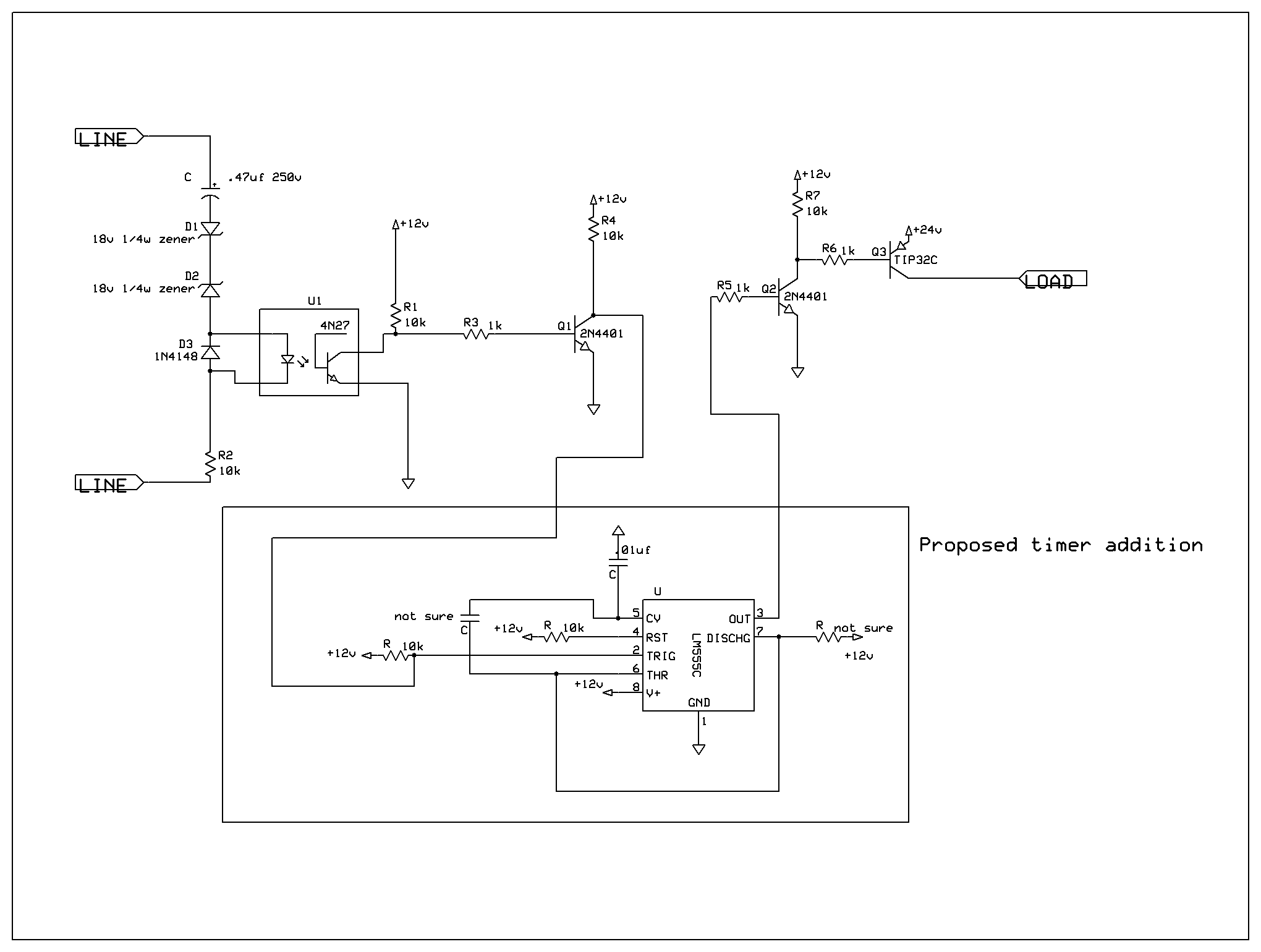
A ringer interface circuit is designed to buffer the output of a central telephone system, which connects to multiple ringers distributed throughout a building. This circuit addresses an issue where the line overloads when ringing, requiring a reset. The intent is to buffer the line, enhancing output capability. However, a problem arises when the circuit is engaged; instead of the expected 24V output, only 12V is observed when the line rings (triggered by the 4N27 opto-isolator). Voltage checks indicate that none of the transistors are fully switching on or off. When the base resistor of the first signal transistor (nearest to the 4N27) is grounded, the output returns to the correct 24V. The schematic text is difficult to read, but it appears that the opto-isolator's output is pulled up to 12V, leading to confusion about the expected 24V output. It is suggested that the output should be lower due to loading through resistor R3 and the base-emitter junction of the left transistor (Q1). There is further discussion regarding the use of a PNP transistor instead of an NPN for Q1 to leverage transistor gain and reduce the current required by the opto-isolator.
The ringer interface circuit serves as a crucial component within a telephone system, facilitating the distribution of ringing signals to multiple endpoints. The design typically includes an opto-isolator, such as the 4N27, which provides electrical isolation between the telephone line and the control circuitry, ensuring that any fluctuations or spikes in the line do not adversely affect sensitive components.
In this configuration, the opto-isolator's output is expected to control the state of a power transistor, often a TIP32, which amplifies the signal to drive the ringers. The original design's failure to achieve the desired 24V output indicates potential issues with the transistor switching characteristics or the loading effects at the output stage. The observation that grounding the base resistor of the first transistor results in the correct output suggests that the preceding stages are not properly biasing the transistors, leading to incomplete switching.
The suggestion to replace the NPN transistor (Q1) with a PNP transistor is notable, as it would allow for better utilization of the power supply and potentially simplify the design by reducing the number of active components. A PNP transistor could be configured to pull the output high more effectively, leveraging the current gain to minimize the load on the opto-isolator.
In summary, the circuit requires careful consideration of the transistor types used, their biasing conditions, and the impact of loading on the output voltage. Adjustments to the schematic and component selection may be necessary to achieve reliable operation and ensure that the system can handle the ringing signals without overload or reset issues.A ringer interface circuit, and I`m running into problems that are over my head. The purpose of the circuit is to buffer the output of a central telephone system that goes to several ringers spaced throughout the building. The reason for the circuit is that whenever the line rings, it overloads and needs to be reset, thusthis circuit will buffer the line and offer a lot more output capability.
Now, my problem is this: when everything is on, and the line is ringing (4N27 triggered), I only get 12V out, instead of 24. I went through and checked voltages, and it seems like none of the transistors are turning on (or off as the case may be) completely.
When I tie the base resistor of the first (closest to the 4N27) signal transistor to ground (turning it 100% off), I then get the correct 24V out. The text on your schematic is so small it`s hard to read, but it looks like the output of the opto is being pulled up to 12V.
Why do you expect 24V there Actually it should be considerably less due to that node being loaded thru R3 and the B-E junction of left transistor (Q1 it`s hard to read). Olin Lathrop Jan 10 `13 at 19:01 I meant the output from the TIP32 power transistor at the end, sorry for the confusion.
Also, I will try and upload a better picture. thanks! Scott Jan 10 `13 at 19:08 It would really make a whole lot more sense if you were to use a PNP at Q1 instead of an NPN. Take advantage of the gain of the transistor to reduce the current that the opto needs to sink. Dave Tweed™ Jan 10 `13 at 19:48 So, in that case, would that mean that since the power transistor is PNP, I could just hook that up instead of Q1, and do away with Q1 & Q2 thanks for the help!
Scott Jan 10 `13 at 20:18 🔗 External reference
