
Optoisolated-high-voltage-driver
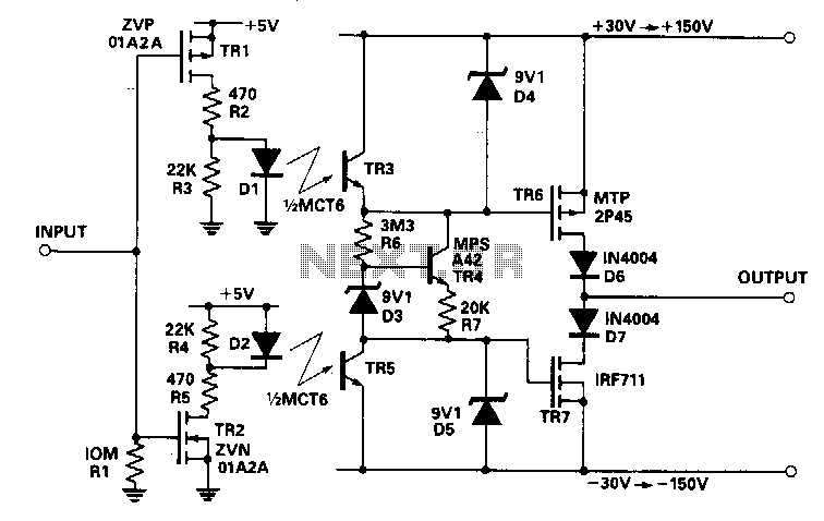
This circuit accepts a signal from a 5-V CMOS logic circuit and produces a high voltage of the same polarity. The high-voltage supply can be adjusted between ±30 V and ±150 V without requiring any changes to the circuit components. The input voltage is connected to the gates of transistors TR1 and TR2. Transistor TR3 is optically coupled to diode D1, while TR5 is coupled to diode D2. Resistor R5 limits the current flowing through D2, whereas resistors R3 and R4 mitigate the effects of leakage current. The light emitted by D1 activates TR3, discharging the gate-source capacitance of TR6, which turns TR6 off. Concurrently, TR5 remains off, and a constant current generated by R6, R7, D3, and TR4 charges the gate-source capacitance of TR7, thereby turning TR7 on. With TR7 activated and TR6 deactivated, the output is drawn close to the lower supply rail. When the input signal is high, TR1 is off, and TR2 is on, which causes D2 to conduct and activate TR5. As TR3 is off and TR5 is on, TR6 turns on, and TR7 turns off, pulling the output towards the higher supply rail.
This circuit operates as a high-voltage level shifter, allowing the conversion of a low-voltage signal from a CMOS logic circuit to a higher voltage level without altering the circuit configuration. The design utilizes a combination of transistors and opto-isolators to achieve this function while maintaining isolation between the low-voltage input and the high-voltage output.
The transistors TR1 and TR2 serve as switches that control the flow of current based on the input signal. When the input is low, TR1 is off, and TR2 is on, allowing the circuit to pull the output towards the lower voltage supply. Conversely, when the input signal is high, TR1 turns off, and TR2 turns on, facilitating the transition of the output towards the higher voltage supply.
Optical isolation is achieved through the use of diodes D1 and D2, which ensure that the high-voltage side of the circuit does not directly interact with the low-voltage logic circuit. This isolation is crucial for protecting sensitive components and ensuring reliable operation.
Resistors R3 and R4 play a vital role in managing leakage currents that could otherwise compromise the performance of the circuit. By limiting these currents, the circuit maintains its integrity and responsiveness.
The configuration allows for a wide range of output voltages, adjustable from ±30 V to ±150 V, which can be beneficial in various applications requiring high voltage levels while still interfacing with standard low-voltage logic circuits. This flexibility, combined with the inherent safety provided by optical isolation, makes the circuit suitable for diverse electronic applications.This circuit takes as an input a signal from a 5-V CMOS logic circuit and outputs a high voltage of the same polarity. The high-voltage supply can be varied from ±30 V to ±150 V without the need to change circuit components.
The input voltage is applied to the gates of transistors TRl and TR2. TR3 is optically coupled to D1 as is TR5 to D2. R5limits the current through D2, while R3 and R4 reduce the affects of leakage current. The light transmitted by Dl turns TR3 on and discharges the gatesource capacitance of TR6, which turns TR6 off. At the same time, TR5 is off and a constant current produced by R6, R7, D3, and TR4 charges the gate-sourced capacitance of TR7, thus turning TR7 on.
With TR7 on and TR6 off, the output is pulled close to the lower supply rail. When the input is high, TRl is off and TR2 is on. Therefore, D2 conducts, which turns on TR5. With TR3 off and TR5 on, TR6 turns on and TR7 off. The output is pulled towards the higher supply rail. 🔗 External reference
Warning: include(partials/cookie-banner.php): Failed to open stream: Permission denied in /var/www/html/nextgr/view-circuit.php on line 713
Warning: include(): Failed opening 'partials/cookie-banner.php' for inclusion (include_path='.:/usr/share/php') in /var/www/html/nextgr/view-circuit.php on line 713