
Parallel-telephone-connection
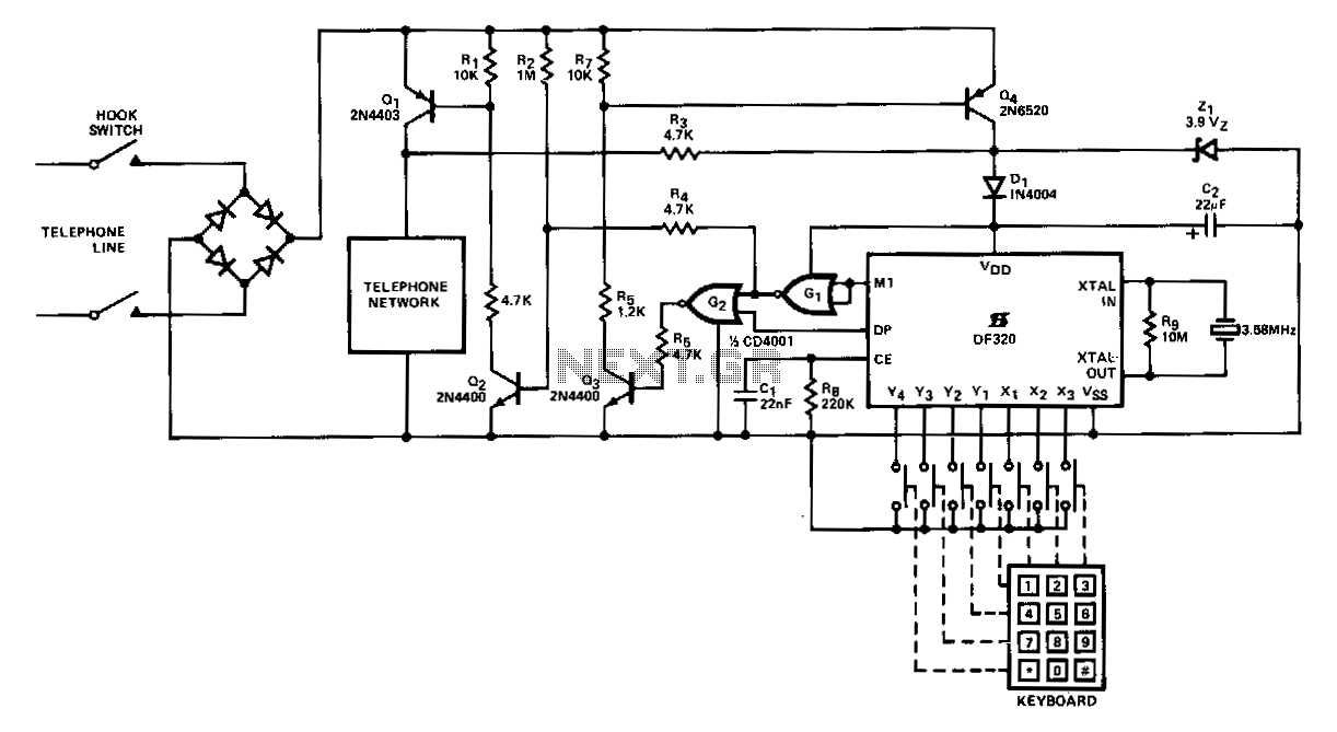
When the handset is lifted and power is applied to the circuit, Q2 receives base current through R2, which subsequently activates Q1. Capacitor C2 charges via resistor R3 in series with diode D1 to a voltage of (Vz1 - 0.7) V. Once the minimum operating voltage is achieved, a power-on reset is initiated through the RC network formed by C1 and R5. Q2 remains in the 'on' state due to the action of G1, while Q3 and Q4 are kept off by G2. The DF320 network presents an impedance greater than 10 kΩ in standby mode, with the telephone network connected through Q1. Upon recognition of the first keyed digit, the DF320 clock is activated. M1 transitions to logic high, causing Q2 and Q1 to turn off, while Q3 and Q4 turn on. Consequently, the majority of the line loop current flows through Q4 and Z1. During impulsing, Q3 and Q4 are deactivated by DP acting on G2, reducing the line loop current to approximately 50 µA through R2, R4, and G2 in series. When dialing, M1 goes to logic low, reconnecting the telephone network. The DF320 then reverts to its static standby condition. If the line loop is interrupted by the cradle switch during dialing, impulsing continues until C2 discharges to a voltage that pulls CE to logic low, resetting the DF320. The diode bridge safeguards the network against line polarity reversal.
This circuit description outlines a telephone interface system utilizing transistors and other components to manage the operation of the telephone line effectively. The system is designed to handle the transition from standby to active states based on user interaction, specifically when the handset is lifted or when digits are dialed.
The operation begins with the lifting of the handset, which applies power to the circuit. Transistor Q2 receives base current through resistor R2, turning it on and subsequently activating transistor Q1. The charging of capacitor C2 through resistor R3 and diode D1 establishes the necessary voltage for the system to function. The voltage (Vz1 - 0.7) V is critical for the proper operation of the circuit.
Once the voltage threshold is reached, the RC network consisting of capacitor C1 and resistor R5 triggers a power-on reset. This reset is essential for ensuring that the circuit starts from a known state. The control signal G1 keeps Q2 in the 'on' state, while transistors Q3 and Q4 remain off, controlled by signal G2. The DF320 network, which operates in parallel with the telephone line, presents a high impedance (greater than 10 kΩ) in standby mode, preventing unnecessary current draw.
The activation of the DF320 clock occurs upon detecting the first digit input by the user. This triggers a change in the logic state of signal M1 to high, which turns off Q2 and Q1, while Q3 and Q4 are turned on, allowing the line loop current to flow predominantly through Q4 and Z1. This configuration is crucial for the operation of the telephone line during dial pulses.
During the dialing process, the system experiences a reduction in line loop current to approximately 50 µA as Q3 and Q4 are controlled by signal DP acting on G2. The reduced current is maintained through resistors R2, R4, and G2 in series, ensuring that the circuit operates within safe limits. Once the dialing is complete, M1 transitions back to a low state, reconnecting the telephone network and allowing the DF320 to return to its standby condition.
In the event of a line loop interruption caused by the cradle switch during dialing, the system is designed to continue the impulsing process until capacitor C2 discharges sufficiently to pull the CE pin to a low logic state, which resets the DF320. This feature ensures that the circuit remains responsive to user inputs and maintains proper functionality.
Additionally, the inclusion of a diode bridge within the circuit serves as a protective measure against line polarity reversal, safeguarding the components from potential damage caused by incorrect connections. This design consideration enhances the reliability and durability of the telephone interface system.When the handset is lifted and power is applied to the circuit, Q2 is fed base current through R2, which in turn drives Ql. C2 is charged via R3 in series with D1 to (Vz1 -0. 7) V. When the minimum operating Vnv voltage is reached, power on reset occurs via the rc network of Cl and RS.
Q2 is maintained in the on condition by Gl, while Q3, and hence Q4, are held off by G2. The DF320 network appears in parallel with the telephone as an impedance more than 10 KO in the standby condition with the telephone network connected in circuit through Ql. On recognition of the first keyed digit, the DF320 clock is started. Ml then goes to logic I causing Q2 and Ql to tum off, and Q3 and Q4 to tum on. Hence, the majority of the line loop current now flows through Q4 and Zl. When impulsing occurs, Q3 and Q4 are turned off by DP acting on G2. Line loop current is then reduced to approximately 50 f"A taken through R2, R4, and G2 in series. When dialing in, complete Ml goes to logic 0, causing the telephone network to be reconnected. The DF320 then returns to the static standby condition. If the line loop is interrupted by the cradle switch during dialing, impulsing will continue until C2 discharges to a voltage, such that R8 pulls CE to logic 0, causing the DF320 to reset. The diode bridge protects the network from line polarity reversal. 🔗 External reference